
|
|
Forum Index : Electronics : all home built solar system
| Author | Message | ||||
| Warpspeed Guru Joined: 09/08/2007 Location: AustraliaPosts: 4406 |
You may possibly need to think about extra components to generate dead time and some fool proof protection against shoot through, especially during power up and power down, and possible brown out conditions, where all the various power supply rails can vary in unpredictable ways with respect to each other. Cheers, �Tony. |
||||
| poida Guru Joined: 02/02/2017 Location: AustraliaPosts: 1389 |
Haxby, yes. In a previous post I mentioned the supply and I wanted to have the choice of 0 - 12V and -12V to 12V, controlled by a 3 pin jumper. I can not resist the chance to do a near optimal comparison of this 2. Warp, I will still use my nanoverter and the IR2184(4). It's a $6 part that gives me the 500nS deadtime. I think I could arrange so that the new design is pin for pin compatible with the previous boards with the 10 pin IDC socket. This will make testing and comparison heaps of fun for me. I think I connect IR2184 VS pin to low side DC ground, VB pin to 12V+ and HO will be DC ground referenced signal of 12V, just like LO. The connections will occur on the powerboard. Brownout and startup conditions have to be studied before I can comment. I agree time has to be spent looking at this stuff. Edited 2021-05-02 18:34 by poida wronger than a phone book full of wrong phone numbers |
||||
| Solar Mike Guru Joined: 08/02/2015 Location: New ZealandPosts: 1123 |
Peter those SI8261BBC-C-IS drivers are great, however if you are wanting to drive multiple mosfets and multiple drivers, the input currents start adding up; OK I guess if powering them all from another half-bridge driver chip. If wanting to use a CPU or other logic output then the UCC5350SB isolated drivers would work better as they have a much higher impedance cmos logic input, just requires the extra supply wire 3.3 - 5v for powering its input side. Mike |
||||
| poida Guru Joined: 02/02/2017 Location: AustraliaPosts: 1389 |
Nicks: I reworked the picoverter PCB in accordance with your guidelines. It made it a lot easier as things got more complex. Also I think the board looks far less messy. 0.3mm tracks is more sensible too. 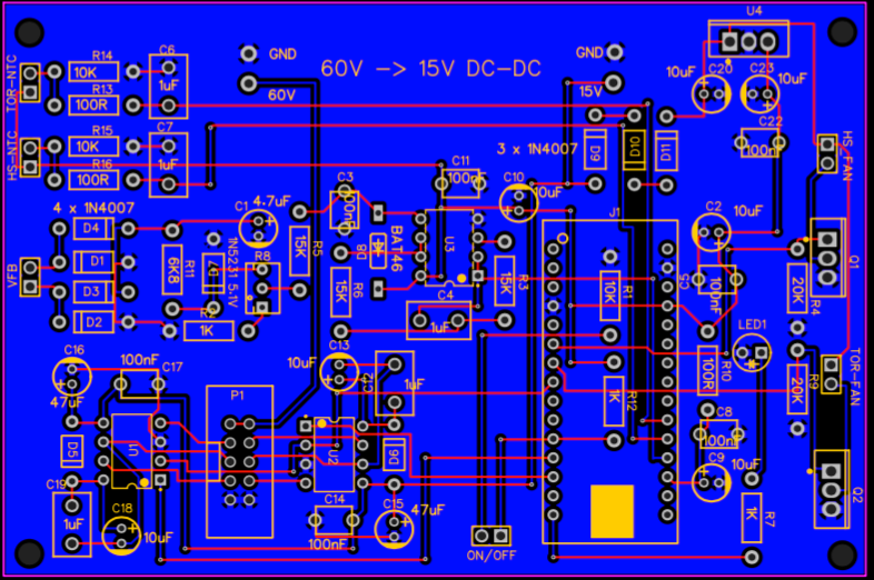 wronger than a phone book full of wrong phone numbers |
||||
| wiseguy Guru Joined: 21/06/2018 Location: AustraliaPosts: 995 |
PCB coming along well. Had a quick look at your schematic. I think Nano Pin 11 should go to pin 2 of the on off header. I think there is a 1u missing from pin 3 of the LM358. I haven't studied it for all errors though. I see you have found the ground plane function - aren't they great ! Edited 2021-05-03 17:56 by wiseguy If at first you dont succeed, I suggest you avoid sky diving.... Cheers Mike |
||||
| poida Guru Joined: 02/02/2017 Location: AustraliaPosts: 1389 |
Thanks Mike for having a look. I think I made an error in the schematic re. on/off header and the 2 resistors. I wanted 10K to pull down to ground at boot time and when not running, i.e. header open. This would sink about 0.5mA to ground. Then I want 5V via 1K (source 5mA) to override the 10K pull down when switch closes. Tomorrow I look at it again with your observations in mind. wronger than a phone book full of wrong phone numbers |
||||
| wiseguy Guru Joined: 21/06/2018 Location: AustraliaPosts: 995 |
It's minor, if you just lift the nano pin 11 connection from pin 1 and place it on pin 2 that will do exactly as you want, with everything else left as is ? The 1u on LM358 pin 3 forms part of the L/P filter network. (Of course this is referring to the schematic, the fix on the PCB might be more complex). Edited 2021-05-04 09:37 by wiseguy If at first you dont succeed, I suggest you avoid sky diving.... Cheers Mike |
||||
| poida Guru Joined: 02/02/2017 Location: AustraliaPosts: 1389 |
Mike, latest schematic and pcb. I completely overlooked the Battery voltage sample and filter which will be needed for LV cut-off. So that's added too. Schematic_picoverter_2021-05-04.pdf PCB_PCB_picoverter 5_2021-05-04(1).pdf How can I check this with fresh eyes? what is the secret? turn it upside down or reverse left to right and then have yet another look? wronger than a phone book full of wrong phone numbers |
||||
| wiseguy Guru Joined: 21/06/2018 Location: AustraliaPosts: 995 |
When I learnt PCB design, you either got a colleague to check your work or you get the PCB back with faults that annoy the crap out of you. With the cost & cycle time that we used to incur it taught you rather quickly to check and recheck. Then I started with a commercial company with deeper pockets, the engineering manager had a mantra of "if you got the PCB back with no errors you spent too much bloody time checking it". He believed there was always going to be something wrong or an unforeseen issue, or an addition of something to make it better, so get your prototype back fast get the bugs etc out of it and then send out a more serious version with most/all bugs ironed out. Today, cycle times and cost are quite minor so the penalty for a mistake is relatively small. I cant see any drastic issues with the PCB or the schematic. You have a generous number of vias and track side changes that a lot could easily be eliminated but it is probably my old school thinking and of minor consequence. What I would try to fix is the tracks that do not enter the component pad at right angles. The creation of sharp angles (less than 90) should be avoided if possible. I'm not familiar with EDA but usually when you set up a snap grid of 25mil and use "hotspot" connect, these off centre exits shouldn't occur ? I was always taught to not use 90 degree changes of direction when running tracks, and use slanting lines (like you have in some areas) again probably old school thinking. Other than that it looks good to go. If at first you dont succeed, I suggest you avoid sky diving.... Cheers Mike |
||||
| Warpspeed Guru Joined: 09/08/2007 Location: AustraliaPosts: 4406 |
I used to agonise over this problem. I know that if there are five errors or omissions lurking in there, and if I spend a week checking I will definitely find four of them ....... eventually. And have to order new boards anyway because of the fifth really dumb mistake. So stuff it !! If one hole size ends up wrong I do not care, I just test the board and fudge whatever needs to be done to make it go. Then I know the second attempt will be perfect. Mike is quite right, the cost and delivery times are now so astoundingly good, its just not worth the anguish. Cheers, �Tony. |
||||
| nickskethisniks Guru Joined: 17/10/2017 Location: BelgiumPosts: 412 |
I'm so glad you guys think the same about those "minor" mistakes. Ok, first of all, excuse me if my English is not coming thru the way I actually want/think and so could misinterpreted, but I don't really want to use it as an excuse, this is the only place to practice my English. With 1000 pages I actually meant it's something interesting to discuss, the longer topics are mostly the interesting ones. What I meant with higher energy is not so the energy needed from the power supply, but the energy needed to charge the gate to make the mosfet turn on or off. When you use a negative bias to hold the mosfet off, you will need to supply more energy to the gate to get the mosfet in on state again. Because you need to go from -5V to +/-4V to have the mosfet turned on, so it will take longer compared to going from 0V to 4V. Unless you use a different gate resistor. The same goes for 15V, if your gate is at 15V, it will take longer (compared to 12V) to have the mosfet in off state again. Of course that's only true if you keep using the same resistors. It's just something to keep in mind. In the last years there were a lot of designs created and a lot of new components and pcb layouts were introduced and used. We are at the stage where it gets very challenging for me to improve things without just copying things from others with consequences. So more time spend on application notes, but also a bit of analyzing other pcb designs, wondering why they did it that way. Different components, for example igbt's and mosfets with their own character/catches, low and higher frequency stuff. Things are not so interchangeable anymore, if this weren't the case already. I had a lot to read up, so I will try to give some interesting input. If you have time to read this, it's an interesting discussion about the importance of a low inductance stage and as Wiseguy suggested, paralleling (with series inductor) different power stages to run 1 load, transformer, motor,.. is something discussed as well. Link I love this forum, but I sometimes go to the suggested forum, you can find a lot of discussion about (motor) inverter/pcb designs. Another approach is having multiple synchronized power stages each with its transformer, and then connecting the secondaries in series. A bit like those cheap HF inverters stepping up the input voltage to a 350VDC bus. But then you come close to the warpverter topology. Wiseguy you are totally right, I think I'm sometimes a bit fanatic if I'm discovering new insights, and sometimes it's just not necessary for example keeping the gate driver as close as possible to the mosfets. The ozzinverter/madpower board proves they don't need it, time will tell. You make very good arguments about the importance about those last nanoseconds, it all doesn't matter when di/dt is slow enough. The Mad power board in combination with the nanoverter is probably the best choice for people that just need a proven design that works when finished. With tht components and simple mechanical structure. That is ok. For me it's important to evolve to perfection although it's not really necessary, for example I want my inverter to start up automatically and displaying the fault or startup sequence . So my wife could use it when needed. That involves some pre charge circuit and output relais, something I want to implement this year, probably (hopefully) used ones in a lifetime. Probably the same story with dedicated turn on/off resistors, it works like it is, so why changing, so sorry if sometimes I'm to pushy about something. Wiseguy did a very beautiful compact layout with the nano power inverter, roll your own style. But I have a small problem with the gatedrive routing, it's running parallel to the battery busbar wich carries a lot of current. This is probably not an issue for his design parameters but when used under verry high load, you can have inductive coupling on the gatewires and potentially cause problems. There is also no separate return path either which is not ideally. But the area between the gate and return path is low, important to make no antenna. Also the resistive path of the power conductors is not symmetric, the inner fets will have a higher current to carry because they are placed closest to the battery and AC terminals. The mosfets on the outside will carry less current. But then again perfectly for his design parameters. This could be easily solved when the ac output terminals were replaced to the outside of the board, this would create an equally path for each mosfet. Sometimes it's just not possible and designing is also looking for a trade of between different things. Wiseguy I hope I didn't offend you. First were some designs I was playing with for a laminated busbar, caps with the right dimension could be placed under the busbar, if the mosfets were placed on an aluminium bar to allow space, like in a design further in this message. The copper could be glued with some solar eva foil, possible creepage issues when voltage to high. You can see a layer of EVA between the + and - plate. Not yet under the AC copper plate. Electrolytics could be placed on the input, compensating the wire between the battery and inverter, the pp should only be there to compensate the pcb inductance? 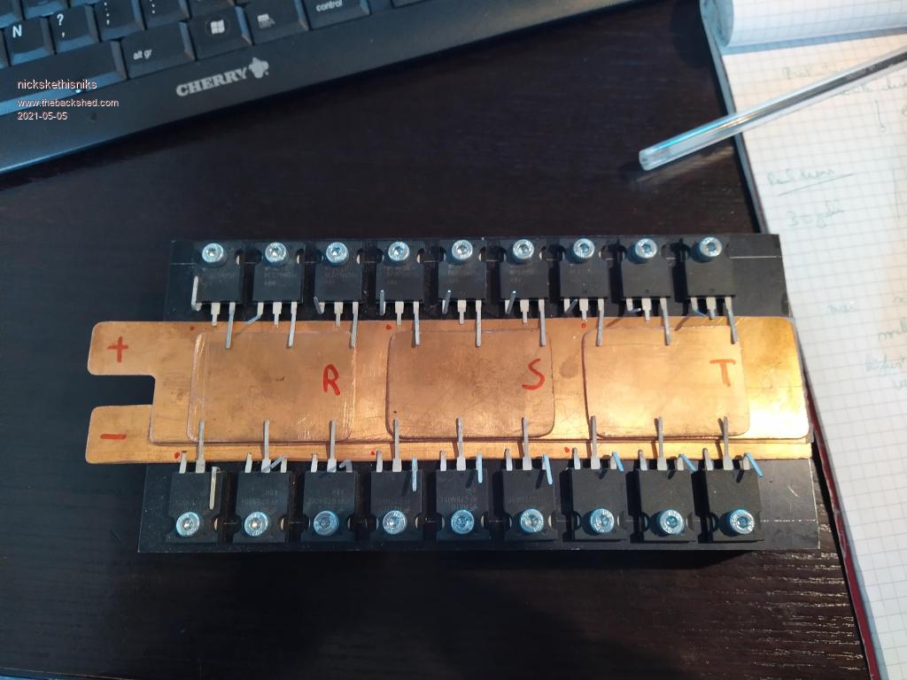 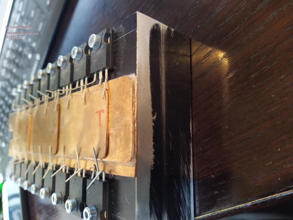 It's also possible with pcb material. 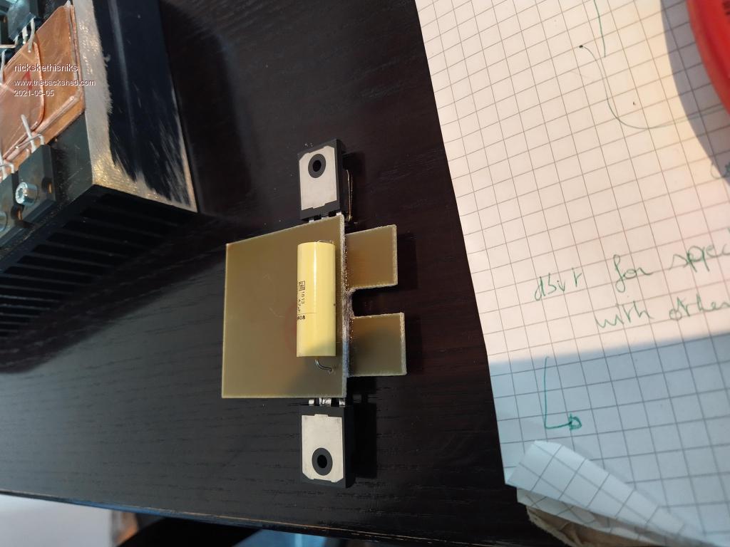 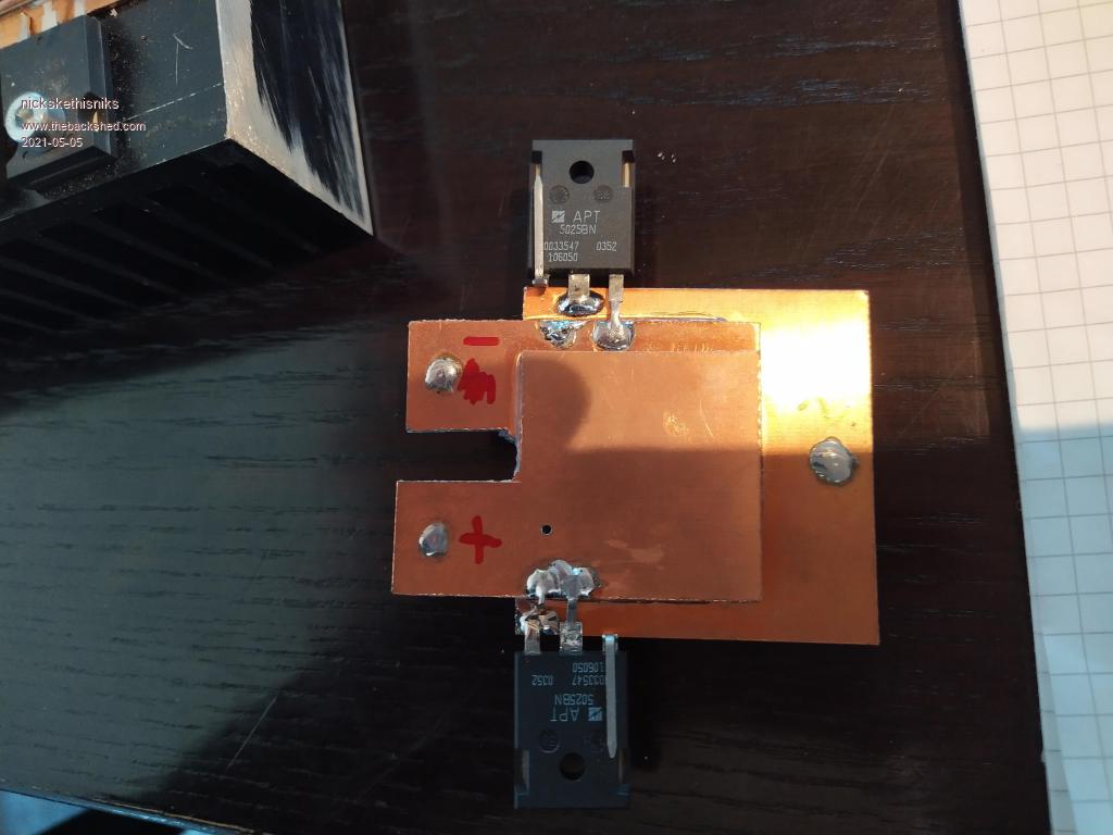 Then I wanted to make a pcb, but I made the mechanical part somewhat complex, if I just had swapped the AC side with the batteryside, it would've been so much easier. I would like to develop a version with mosfets on the other side of the board. It's already some time ago but here are some examples I was (wanted) playing with. So in the meantime there are things to improve. I'm still searching, maybe we can find something togheter. 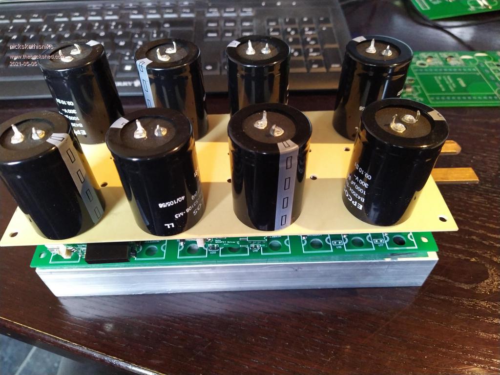 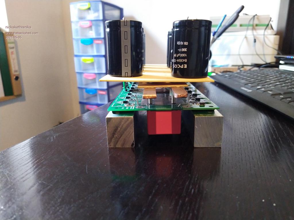 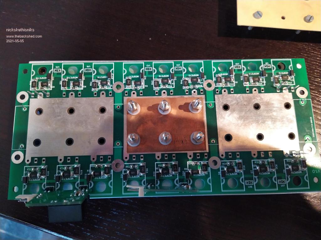 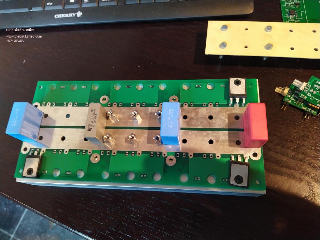 The same board but the fets on top: 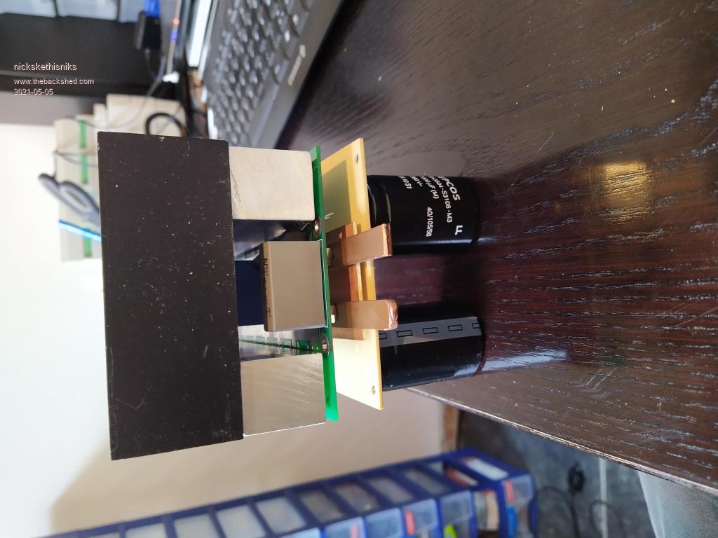 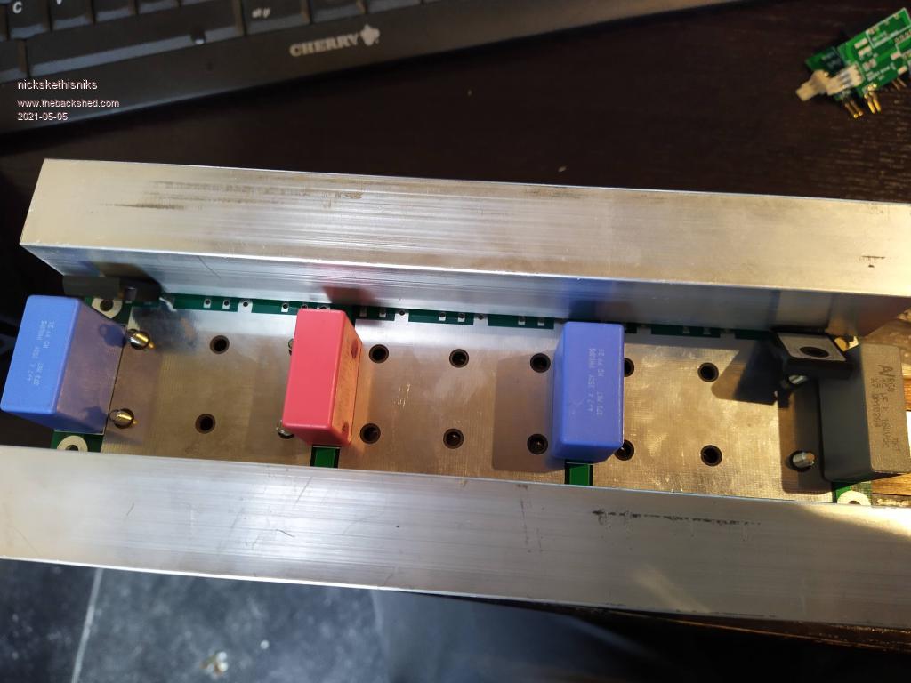 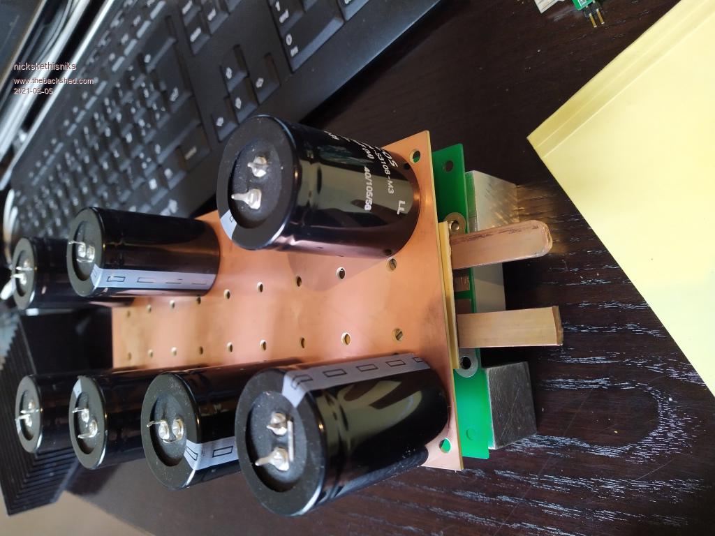 This was the little driverboard: maybe that ground plane is not necessary, a separate driver board gives some space on the board itself, placed under 90degree with the power tracks should make it more immune against noise. And makes experimenting easy. You can easily fit an totem pole drive on such a pcb. 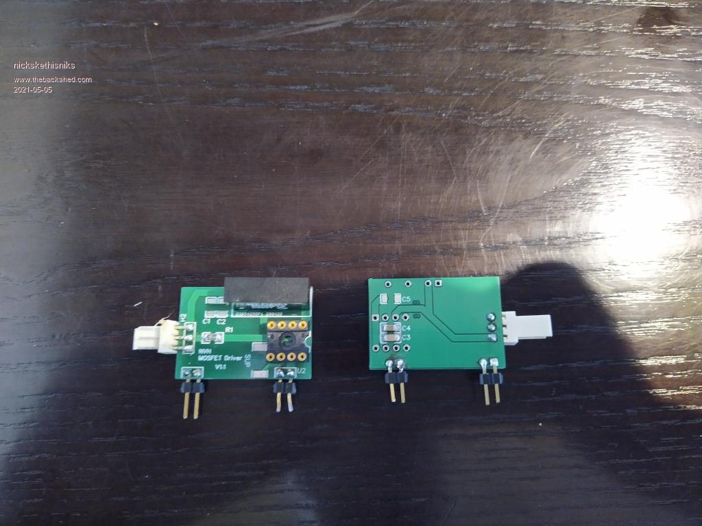 Peter this is maybe how you could place the mosfetdriver, I could've used smaller resistors. 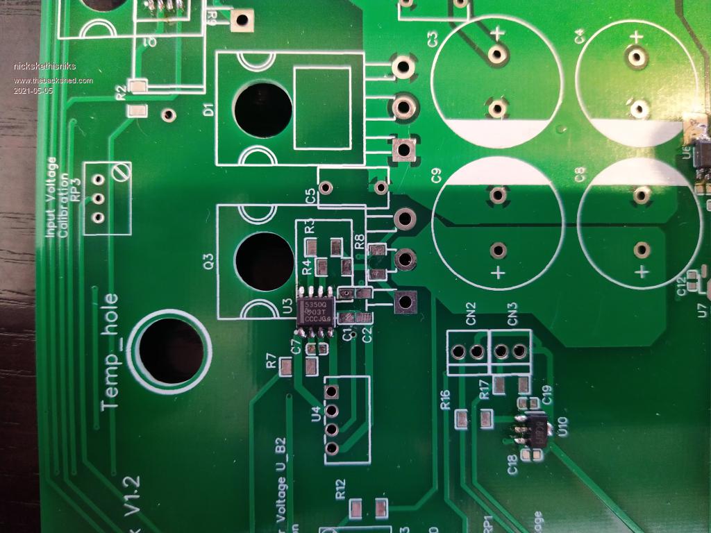 Edited 2021-05-05 01:10 by nickskethisniks |
||||
| wiseguy Guru Joined: 21/06/2018 Location: AustraliaPosts: 995 |
When I batched all my FETs for on resistance I installed ones with the higher on resistance closer to the centre and the ones with less to the outside - you shouldn't make too many assumptions without being in possession of all the facts, you might be surprised at the lengths I go to in my attempts to get things right. I find it hard to fathom why you are cherry picking what you consider faults or issues with my design, which I might add worked first time, has never blown a FET & has one of the best gate drive results published on this forum to date, and at 2kW output runs a few degrees above ambient with no fan. It also now has the automatic precharge/soft start that I was so canned for when I first suggested it. I cannot agree with you that the MAD board is definitely the way to go, there were valid reasons why I did not copy it (probably similar reasons as to why you are designing a totally different approach). I applaud the fact that there are a number out there working well & for long periods but it seems sometimes they can go bang for unexplained reasons sometimes multiple times before they behave. You are suggesting theoretical and possible perceived issues of my design which are not actual issues that I have seen any evidence of. The difference in energy and time to go from -5 to + 12 compared to 0-12 is negligble. Do the sums: delta 5V 30nF 10A+ of drive current 2R2 resistor no miller effect to fight until you get to ~ 5V positive and we are talking at most a handful of nanoseconds. In the data sheet with a 6ohm resistor and 10V gate drive, the turn on delay was 28nS and the rise time 18nS whilst fighting 40V of Miller through ~ 1nF. If 1A flows for 1 second we have 1 coulomb, the gate charge of the HY4008 is 200nano coulombs 1/5,000,000 of a coulomb by my sums. Even at 20kHz switching I think that translates to ~ 5mA ? I will read the rest of your post more carefully in the morning it is after 2.30am and I'm turning in now. If at first you dont succeed, I suggest you avoid sky diving.... Cheers Mike |
||||
| nickskethisniks Guru Joined: 17/10/2017 Location: BelgiumPosts: 412 |
Maybe we better start a new thread? Peter I don't want to pollute your thread or is it allright? Sorry I am cherry picking, you are right, I knew I was on slippery ice when I was looking at your design thru a magnifier. Next time I will change my tone by asking you why you made certain decisions instead of making assumptions, sorry, I must have overlooked it in your building thread. I was trying to examine your pcb layout based on the things I've read and learned so far. That way learning the do's and don'ts, ok, you however, you have the ability to bent the theoretical rules on a clever way by using a disadvantage, for instance the internal resistance deviation, in your favor. I'm in the stage to interpret the theoretical rules and trying to implement them, I know practice turns out differently because of compromises you need to make. Today I learned something new, I don't have the experience you have, I'm building my knowledge and making my notes. But for starting it's good practice to start with a symmetric layout. I also know there are other aspects that contribute to the current sharing, temperature for instance will probably work in our favour. Does anyone have the complete pcb layout from the madinverter power pcb? I would like to think about how it could be made better. I didn't say it is the way to go for starters, but probably the best choice of what you can get at the moment if you want to start. I think there were no other designs open source that well documented, besides the ozzinverter. Does anyone have the complete pcb layout from the madinverter power pcb? I would like to think about how it could be made better. I can't find it. Here there is a link to the version without the totem pole driver: https://www.thebackshed.com/forum/ViewTopic.php?TID=8807&P=5 https://www.thebackshed.com/forum/uploads/Madness/2018-05-03_220947_2018-02-16_025148_EXP_POWER_BOARD_SCHEMATIC_P1.pdf I did find the 2 other application notes back in my OneNote. Parasitic oscillation and ringing of power mosfets (Toshiba) Toshiba Fundamentals of mosfet and igbt gate driver circuits (Texas instruments) Texas instruments And 3 others contributed by: By solarmark Infineon Irf By madness: Infineon Edited 2021-05-05 07:10 by nickskethisniks |
||||
Haxby Guru Joined: 07/07/2008 Location: AustraliaPosts: 418 |
Good to see lots of people tackling the same problems in different ways. And it's good to see higher power automotive designs where all the nuances are amplified. The Chinese boards use a piece of copper dipped in solder to create a PCB based bus bar. I tried that approach on my boards but wasn't very happy with it. Looks messy. I like your stacked busbar design nickskethisniks. If we design a board for other members to recreate, maybe basing the busbars on easy to get materials could be a focus. I picked up some bus bars that are commonly available world-wide in the electrical trade. These copper pre-cut and bent bars are marketed to connect multiples of single DIN rail modules (breakers) together quickly instead of wires. They are rated at 63A for that purpose. I'm contemplating a redesign of my power board to use these busbars and maybe others here could consider them to fortify their high current PCB tracks. 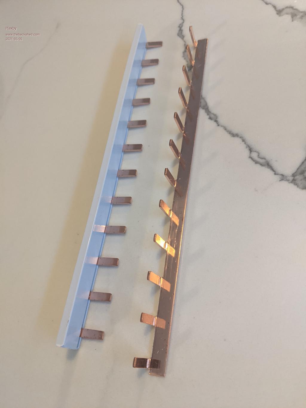 |
||||
| wiseguy Guru Joined: 21/06/2018 Location: AustraliaPosts: 995 |
Nicks, I have watered down my response & extend an olive branch and accept your apology. I don't mind answering questions or/and criticism publicly if I have stuffed up - I'm not infallible either. The first statement seemed to infer your strong support of the MAD design. I also apolgise to Peter for the unintended "pollution" but ignoring any negativity the design approach discussion has some good food for thought & ideas coming out. One could infer that in the one post by promoting the Mad design, displaying your design approach and drawing negative attention to and suggesting my design approach seemed to have multiple flaws is not a great approach to take in a public forum, and I objected. I think you knew by saying "I hope that I haven't offended you" it was probably not going to be received well. Your suggestion that the supply busbar energy may transfer to the gate wire does not take into consideration that on the other side of the gate trace, the AC terminal return bus carries equal and opposite energy along the same length back to the AC terminal, that should cancel out any induced signal. Proposing to move the AC terminal to the end could only have a negative effect. I also like your thinking outside the square approach to FET high current stage design and I do strongly support input of fresh and novel ideas. It is a shame that with the other content on your post it drew attention away from your good ideas & got less attention than it deserved. End of pollution .... normal channel content can now resume. I considered the copper bus bar approach of Haxbys when trying to exploit 1oz PCBs. I was too lazy/uninspired to go and get a decent length to play with but I did get a small sample from the fellow that wired up my 3 phase to the workshop. Its only downfall is that it tells you where it will go with its regular "feet" but to design in from go I still think it has a lot of merit & I will probably use it at some stage. The insulated cover is also a big plus to help keep you out of trouble when probing measurements whilst building/testing and can maybe be removed to assist against heat build up when commissioned ? Lengths of vertical PCB strips with appropriate feet at regular intervals is another way of exploiting cheap PCB manufacture to our advantage. Edited 2021-05-07 12:53 by wiseguy If at first you dont succeed, I suggest you avoid sky diving.... Cheers Mike |
||||
| Solar Mike Guru Joined: 08/02/2015 Location: New ZealandPosts: 1123 |
Poida, I would like to use your picoverter to drive a 100v H-Bridge that I am currently designing, and have a question about the driver signals it outputs to the mosfet power board. The VS1-Drv signal going to U1 (HO1,LO1) and VS2-Drv to U2, is one chip purely 20Khz spwm and the other 50Hz binary; or do you do some fancy switching inside the CPU to swap the spwm and 50Hz drive signals over every 100HZ so each chip shares the spwm. Cheers Mike |
||||
| Warpspeed Guru Joined: 09/08/2007 Location: AustraliaPosts: 4406 |
While we are kicking around a few ideas for hardware layout, this is the very last PWM inverter I built, just over three years ago. Its now become a pretty dated design, in that it uses an old EGS board, but this was just a design exercise to try out a few different mechanical and thermal construction ideas. It also uses four ten amp gate driver chips mounted up fairly close to each pair of mosfets. Each chip has short direct gate connections to each pair of mosfets in an attempt to get cleaner more direct gate drive signals as discussed in this thread. It also bears a slight resemblance to Nicks laminated busbar idea. Not quite so neat, but it uses busbars bolted to the circuit board to carry the heavy current. This is the dc side with +ve and -ve busbars and the single low esr electrolytic. 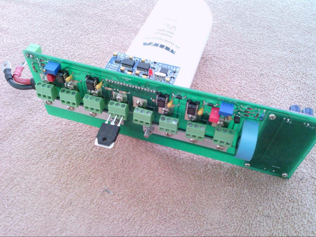 The ac side busbars cross over. 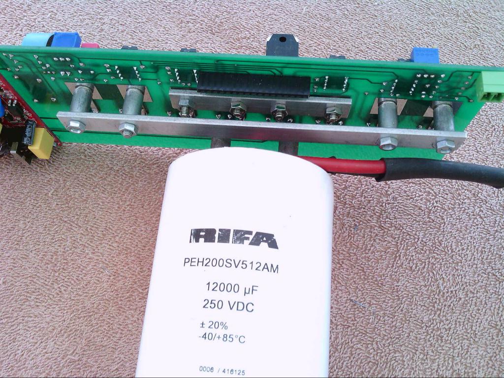 Its only a one ounce board, but source and drain connections are reinforced with solder lugs, so that if it ever blows up the pcb tracks are just about indestructible 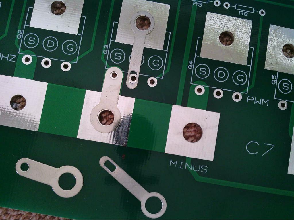 Installed in a metal enclosure with still only half the mosfets installed. The mosfets are inside, but the heatsink is outside the enclosure. 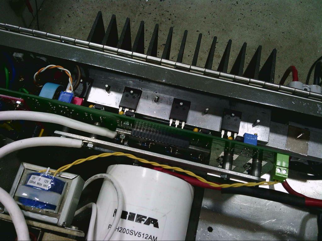 A large piece of 6mm thick L section conducts the heat to the outside heatsink. That seemed to work quite well. 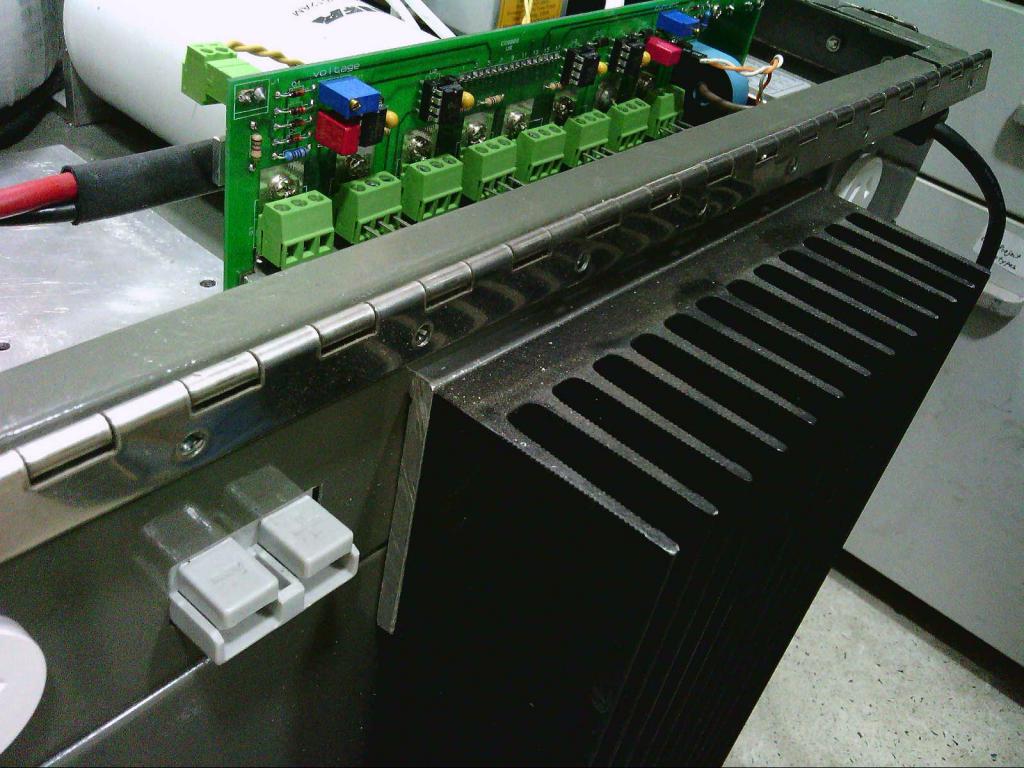 I don't know if any of this is of any interest to anyone, or even relevant, but I thought it might spur a few ideas. Cheers, �Tony. |
||||
| Solar Mike Guru Joined: 08/02/2015 Location: New ZealandPosts: 1123 |
Looks very professional, how well did those drivers (TC4452 comes to mind) work driving two mosfets. Cheers Mike |
||||
| Warpspeed Guru Joined: 09/08/2007 Location: AustraliaPosts: 4406 |
Its not something I spent a lot of time looking at, but the gate waveforms looked fine from what I can remember. Sorry, but I never recorded a picture of that. Cheers, �Tony. |
||||
| poida Guru Joined: 02/02/2017 Location: AustraliaPosts: 1389 |
It runs code that does the fancy switching. at some point in time: U1 drives LOW side FETS on, pulling VS1 to ground. U2 drives a SPWM 1/2 wave using LOW and HIGH side FETS. then, the roles are switched. Now U2 drives LOW side FETS on, pulling VS2 to ground. And U1 does the SPWM with LOW and HIGH side FETS driving VS1 I did have code that mimicked the EG8010. But after a prod from Wiseguy I made the above code and it works as good if not a little better than EG8010. Edited 2021-05-09 16:16 by poida wronger than a phone book full of wrong phone numbers |
||||
