
|
|
Forum Index : Microcontroller and PC projects : Sprint Layout
| Author | Message | ||||
| Mixtel90 Guru Joined: 05/10/2019 Location: United KingdomPosts: 5730 |
DesignSpark is a more versatile package than Diptrace, I think (up to 14 layers and 1m square IIRC). I'm playing with DesignSpark at the moment and I've done a very simple board. I *had* to mess with the colours and font though, and I'm still not happy with some of the things (Rotate a schematic component and the labels etc. rotate with it? urgh... That's so 1970's). Creating custom libraries and components seems to be a lot easier than KiCAD. That's a relief because I don't think I can live with some of them. lol Setting the browser to use a white list of sites that can drop cookies gave me a degree of satisfaction. :) Mick Zilog Inside! nascom.info for Nascom & Gemini Preliminary MMBasic docs & my PCB designs |
||||
| Tinine Guru Joined: 30/03/2016 Location: United KingdomPosts: 1646 |
Holy moly!  Craig |
||||
| Solar Mike Guru Joined: 08/02/2015 Location: New ZealandPosts: 1123 |
I use Diptrace extensively (paid for non profit full version), I think its by far the easiest PCB and Schematic design package out there for the price. Making custom libraries and components is fast and intuitive. If you are doing a lot of boards its best to purchase the product than rely on knobbled cut down versions. Mike |
||||
| Tinine Guru Joined: 30/03/2016 Location: United KingdomPosts: 1646 |
Yeah, I just pulled-in a Parallax DipTrace schematic and ran the Autorouter.....NICE!!!  Craig |
||||
| Mixtel90 Guru Joined: 05/10/2019 Location: United KingdomPosts: 5730 |
The minimum Diptrace is $75 now, with a limit of 2 layers and 300 pins. The Lite version is $145 for 2 layers and 500 pins. Regular is $395 for 4 layers and 1000 pins. I couldn't justify those prices now, I'm afraid, even if it is excellent software. KiCAD probably beats it on specification and reliability (it's been around for a long time now) and is free (but has a steep learning curve). SL is less than 50 euros, does 4 layers and has no pin limit or board size limit that I can find. I suppose you run out of memory at some point. If I can eventually get the hang of DesignSpark that will be a lot more than enough for me - and costs nothing. Mick Zilog Inside! nascom.info for Nascom & Gemini Preliminary MMBasic docs & my PCB designs |
||||
lew247 Guru Joined: 23/12/2015 Location: United KingdomPosts: 1676 |
Easyeda Is dead simple to use, simple and free You can use it all online or download it and after checking for no errors you can upload the design direct to JLPCB for manufacturing |
||||
| Tinine Guru Joined: 30/03/2016 Location: United KingdomPosts: 1646 |
It's all great stuff. Right now, I'm not worried with my large board. SL is doing a great job. 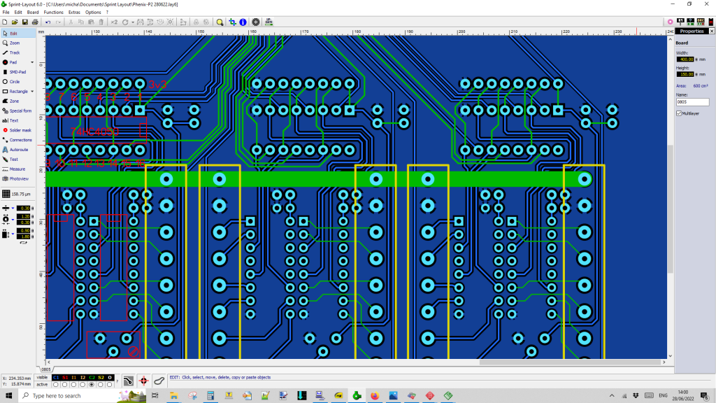 Craig |
||||
| Mixtel90 Guru Joined: 05/10/2019 Location: United KingdomPosts: 5730 |
Yay! I've created a PicoMite in DesignSpark without going any crazier than I was before! (Well, I don't think so...) That's looking pretty, Craig. Be careful about the minimum track sizes and clearances that your chosen PCB house can handle. That applies to the width of lines used to draw silk screen characters too. I generally set the minimum to 0.15mm and normally work with a track width of 0.4mm if I can, which can carry about 1.4A using 1oz copper (best to derate it a little). Also, on a big board, make sure there is plenty of support or thin traces might break if it flexes. It may even be worth going for 2mm board rather than 1.6mm. Mick Zilog Inside! nascom.info for Nascom & Gemini Preliminary MMBasic docs & my PCB designs |
||||
| Tinine Guru Joined: 30/03/2016 Location: United KingdomPosts: 1646 |
Thanks Mick. We definitely think alike. I have always been thinking about the 2mm board and I need to get some screw holes around the 12-way connectors because they really need some oomph to pull apart. Board flex has been a consideration from the get-go Craig |
||||
| pwillard Senior Member Joined: 07/06/2022 Location: United StatesPosts: 274 |
But, ummmm... this thread was supposed to be *about* Sprint Layout. :-P |
||||
| lizby Guru Joined: 17/05/2016 Location: United StatesPosts: 3015 |
If the OP himself participates in the straying off-topic (so common here, and often so informative), who's to grouse? PicoMite, Armmite F4, SensorKits, MMBasic Hardware, Games, etc. on fruitoftheshed |
||||
| Mixtel90 Guru Joined: 05/10/2019 Location: United KingdomPosts: 5730 |
But I'd already created a PicoMite in Sprint Layout (the stamp version as well). I needed a challenge. :) :P Edited 2022-06-29 00:39 by Mixtel90 Mick Zilog Inside! nascom.info for Nascom & Gemini Preliminary MMBasic docs & my PCB designs |
||||
| pwillard Senior Member Joined: 07/06/2022 Location: United StatesPosts: 274 |
well, I was poking fun ;-P It does seem a number of us like making PCB's. I claim that it is therapeutic... like puzzle solving. |
||||
| Tinine Guru Joined: 30/03/2016 Location: United KingdomPosts: 1646 |
Isn't it just Craig |
||||
| Mixtel90 Guru Joined: 05/10/2019 Location: United KingdomPosts: 5730 |
Agreed, it is. Especially if you are routing the board manually. I have noticed though that DesignSpark seems to like to add a via or two when autorouting - even when they aren't needed. I've always said that you can't trust computers. :) Mick Zilog Inside! nascom.info for Nascom & Gemini Preliminary MMBasic docs & my PCB designs |
||||
| Tinine Guru Joined: 30/03/2016 Location: United KingdomPosts: 1646 |
Here ya go Mick.... |
||||
| Mixtel90 Guru Joined: 05/10/2019 Location: United KingdomPosts: 5730 |
See? I have words of wisdom. :) Unhappy memories of swapping 81LS97 chips round on Nascom PCBs because some seemed to work in positions where others wouldn't. We couldn't trust the hardware, never mind the software. :( Mick Zilog Inside! nascom.info for Nascom & Gemini Preliminary MMBasic docs & my PCB designs |
||||
| Mixtel90 Guru Joined: 05/10/2019 Location: United KingdomPosts: 5730 |
Something that no-one has mentioned so far in this thread is that Sprint Layout has a Gerber import facility. You can (usually) rebuild a board from its Gerber files, edit it and produce your own variation. It doesn't produce the circuit diagram for you, obviously, but you have the silkscreen layers, which can be very helpful. Mick Zilog Inside! nascom.info for Nascom & Gemini Preliminary MMBasic docs & my PCB designs |
||||
| pwillard Senior Member Joined: 07/06/2022 Location: United StatesPosts: 274 |
You can use the Gerber imports... but editing the result is a more complicated experience. One downside to the Gerber import is that it creates FILL areas using roughly 0.5 tracks... so you pretty much end up needing to remove the "fills" manually to make any sense of the board (if you need to modify it). You may also need to play around with item grouping since parts aren't "parts" anymore... everything is essentially an "art" object. (Understandable since GERBER is a "graphical" file format) |
||||
| matherp Guru Joined: 11/12/2012 Location: United KingdomPosts: 8584 |
That's because it is a really really bad idea  |
||||
