
|
|
Forum Index : Microcontroller and PC projects : ARMmite - first general beta release
| Author | Message | ||||
| matherp Guru Joined: 11/12/2012 Location: United KingdomPosts: 11512 |
Hi all please find attached a hex file for the first general beta release of the ARMmite. This is the Micromite MKII v4.6b firmware ported to the STM32F407VG chip with some small changes and some enhancements which I will detail below. Please remember this is an early beta so there will be bugs, please PM me as and when you find them To get started with this the easiest way is to buy one of the STM32F4DISCOVERY boards. This contains all that is needed to program the firmware into the microcontroller and gives access to all of the I/O pins. Even better it is very cheap  , typically around �12 in the UK. , typically around �12 in the UK.
It is important to get the STM32F407VG version of the board. This can be obtained from RS (part number 745-8434) or Farnell (Order Code: 2009276) amongst other places. Don't buy the STM32F429 version of the board even though it looks sexier - the firmware won't work. 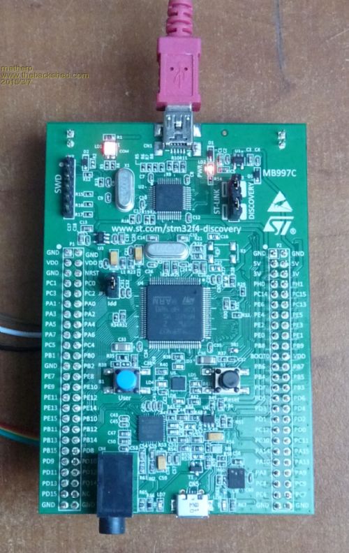
So why do you want to do this? First, the ARMmite runs up to 4x faster than the PIC32MX170 Second, it has lots more memory for programs and for data Third, it has lots more pins (80 I/O pins available to the user) Fourth, it has new facilities including two SPI ports, two 12-bit DACs and fourteen 12-bit ADCs Fifth, it is new and we all like new toys Sixth, it is really cheap (did I already say that?) To program the firmware into the chip you need to download and install the STM ST-LINK utility software Then plug the Discovery board into a USB port on your PC, load up the firmware and program it into the chip. Leave the USB cable plugged in to provide power to the Board. 2015-03-07_155035_STM32B10.zip You then need to connect a standard USB to TTL converter to the console pins on the discovery board. GND on the TTL adapter goes to any of the GND pins on the discovery board RX on the adapter goes to PA2 on the discovery board TX on the adapter goes to PA3 on the discovery board Then open up a terminal on your PC (Teraterm or MMEdit) and connect to the appropriate serial port for the TTL adapter (38400 baud) - exactly the same as for a normal Micromite. Click the Reset button on the discovery board and you will get the ARMmite copyright message and the command prompt - you are then up and running. 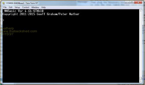
I use MMEdit to develop and download programs - set MMEdit to Micromite MKII mode. Alternatively you can use the EDIT command from the console, exactly the same as the normal Micromite. I will be producing an updated version of Geoff's Micromite manual to fully detail the ARMmite, but in the meantime here are the key current differences: The PWM and SERVO commands are now enhanced by making 4 channels available on each timebase so: PWM 1,10000,20,40,60,80 And SERVO 2,1.44,1.66,1.88,2.22 are both valid. This means up to 8 servos could be controlled at once. Com2: is now a full hardware USART rather than being implemented in SW so speeds upto 115200 are valid. In the case of both comm ports; the buffer size parameter in the OPEN command is not implemented � this is set at 2048 bytes. Also, the data format is set at 8bits, 1 stop bit, normal polarity, normal push-pull output. IEEE 485 is not implemented on either port. The LOF() function now returns the number of spaces left in the comm receive buffer, rather than the transmit buffer, transmit is now blocking. Two 12-bit DACs are available through Basic. the Command syntax is: DAC number,voltage ' number can be 1 or 2, voltage is a float between 0 and 3.3v DAC number,STOP ' turn off the DAC The CPU command and the WATCHDOG command are not implemented, CPU speed is fixed at 168MHz I2c works as per the micromite manual with the following restrictions: I2c slave mode is not implemented. I can�t see any reason to use a comparatively expensive 100-pin chip as an i2c slave (that is what picaxes or the 28-pin MX170 are for!). 10-bit addressing mode is not implemented � I personally have never seen a device that uses a 10-bit address. Option baudrate nnnn works, however this only comes into effect on the next restart � seems more logical than happening immediately. SPI OPEN; you can no longer set the bit length, it is always 8-bits. Just output 2 or 4 bytes to achieve the same as setting the bit length to other than 8 Command is now �SPI OPEN speed,mode� valid speeds are 165,000 to 42,000,000 SPI2 OPEN, SPI2 WRITE, SPI2 READ, n=SPI2(m) are implemented to enable a second SPI channel. �SPI2 OPEN speed,mode� valid speeds are 83,000 to 21,000,000 The various OPTION CONSOLE commands are not implemented. OPTION CLOCKTRIM is not required as the microcontroller uses an external crystal. OPTION PIN is not currently implemented Data Cfunctions can be used as for the Micromite MkII, program Cfunctions are not yet implemented. The pinout for the chip is: PE2, DIGITAL_IN | DIGITAL_OUT | OC_OUT | COUNT // pin 1 PE3, DIGITAL_IN | DIGITAL_OUT | OC_OUT | COUNT // pin 2 PE4, DIGITAL_IN | DIGITAL_OUT | OC_OUT | COUNT // pin 3 PE5, DIGITAL_IN | DIGITAL_OUT | OC_OUT | IR // pin 4 PE6, DIGITAL_IN | DIGITAL_OUT | OC_OUT // pin 5 // pin 6 - VBAT PC13, DIGITAL_IN | DIGITAL_OUT | OC_OUT // pin 7 PC14, DIGITAL_IN | DIGITAL_OUT | OC_OUT // pin 8 PC15, DIGITAL_IN | DIGITAL_OUT | OC_OUT // pin 9 // pin 10 - VSS // pin 11 - VDD // pin 12 - External Xtal // pin 13 - External Xtal // pin 14 - NRST PC0, ANALOG_IN | DIGITAL_IN | DIGITAL_OUT | OC_OUT // pin 15 PC1, ANALOG_IN | DIGITAL_IN | DIGITAL_OUT | OC_OUT // pin 16 PC2, ANALOG_IN | DIGITAL_IN | DIGITAL_OUT | OC_OUT // pin 17 PC3, ANALOG_IN | DIGITAL_IN | DIGITAL_OUT | OC_OUT // pin 18 // pin 19 - VDD // pin 20 - VSSA // pin 21 - VREF+ // pin 22 - VDDA PA0, ANALOG_IN | DIGITAL_IN | DIGITAL_OUT | OC_OUT // pin 23 PA1, ANALOG_IN | DIGITAL_IN | DIGITAL_OUT | OC_OUT // pin 24 PA2, Console TX // pin 25 // PA3, Console RX // pin 26 // pin 27 - VSS // pin 28 - VDD PA4, ANALOG_IN | DIGITAL_IN | DIGITAL_OUT | OC_OUT // pin 29 PA5, ANALOG_IN | DIGITAL_IN | DIGITAL_OUT | OC_OUT // pin 30 PA6, ANALOG_IN | DIGITAL_IN | DIGITAL_OUT | OC_OUT | PWM2A // pin 31 PA7, ANALOG_IN | DIGITAL_IN | DIGITAL_OUT | OC_OUT | PWM2B // pin 32 PC4, ANALOG_IN | DIGITAL_IN | DIGITAL_OUT | OC_OUT // pin 33 PC5, ANALOG_IN | DIGITAL_IN | DIGITAL_OUT | OC_OUT | PWM2C // pin 34 PB0, ANALOG_IN | DIGITAL_IN | DIGITAL_OUT | OC_OUT // pin 35 PB1, ANALOG_IN | DIGITAL_IN | DIGITAL_OUT | OC_OUT | PWM2D // pin 36 PB2, DIGITAL_IN | DIGITAL_OUT | OC_OUT // pin 37 PE7, DIGITAL_IN | DIGITAL_OUT | OC_OUT // pin 38 PE8, DIGITAL_IN | DIGITAL_OUT | OC_OUT // pin 39 PE9, DIGITAL_IN | DIGITAL_OUT | OC_OUT // pin 40 PE10, DIGITAL_IN | DIGITAL_OUT | OC_OUT // pin 41 PE11, DIGITAL_IN | DIGITAL_OUT | OC_OUT // pin 42 PE12, DIGITAL_IN | DIGITAL_OUT | OC_OUT // pin 43 PE13, DIGITAL_IN | DIGITAL_OUT | OC_OUT // pin 44 PE14, DIGITAL_IN | DIGITAL_OUT | OC_OUT // pin 45 PE15, DIGITAL_IN | DIGITAL_OUT | OC_OUT // pin 46 PB10, DIGITAL_IN | DIGITAL_OUT | OC_OUT | comm1 TX // pin 47 PB11, DIGITAL_IN | DIGITAL_OUT | OC_OUT | comm1 RX // pin 48 // pin 49 - VCAP1 // pin 50 - VDD // PB12, DIGITAL_IN | DIGITAL_OUT | INTERRUPT | OC_OUT // pin 51 PB13, DIGITAL_IN | DIGITAL_OUT | OC_OUT | SPI2CLK // pin 52 PB14, DIGITAL_IN | DIGITAL_OUT | OC_OUT | SPI2IN // pin 53 PB15, DIGITAL_IN | DIGITAL_OUT | OC_OUT | SPI2OUT // pin 54 PD8, DIGITAL_IN | DIGITAL_OUT | INTERRUPT | OC_OUT // pin 55 PD9, DIGITAL_IN | DIGITAL_OUT | INTERRUPT | OC_OUT // pin 56 PD10, DIGITAL_IN | DIGITAL_OUT | INTERRUPT | OC_OUT // pin 57 PD11, DIGITAL_IN | DIGITAL_OUT | INTERRUPT | OC_OUT // pin 58 PD12, DIGITAL_IN | DIGITAL_OUT | OC_OUT // pin 59 PD13, DIGITAL_IN | DIGITAL_OUT | OC_OUT // pin 60 PD14, DIGITAL_IN | DIGITAL_OUT | OC_OUT // pin 61 PD15, DIGITAL_IN | DIGITAL_OUT | OC_OUT // pin 62 PC6, DIGITAL_IN | DIGITAL_OUT | OC_OUT | comm2 TX // pin 63 PC7, DIGITAL_IN | DIGITAL_OUT | OC_OUT | comm2 RX // pin 64 PC8, DIGITAL_IN | DIGITAL_OUT | OC_OUT // pin 65 PC9, DIGITAL_IN | DIGITAL_OUT | OC_OUT // pin 66 PA8, DIGITAL_IN | DIGITAL_OUT | OC_OUT // pin 67 PA9, DIGITAL_IN | DIGITAL_OUT | OC_OUT // pin 68 PA10, DIGITAL_IN | DIGITAL_OUT | OC_OUT // pin 69 PA11, DIGITAL_IN | DIGITAL_OUT | OC_OUT // pin 70 PA12, DIGITAL_IN | DIGITAL_OUT | OC_OUT // pin 71 PA13, DIGITAL_IN | DIGITAL_OUT | OC_OUT // pin 72 // pin 73 | VCAP2 // pin 74 | VSS // pin 75 | VDD // PA14, DIGITAL_IN | DIGITAL_OUT | OC_OUT // pin 76 PA15, DIGITAL_IN | DIGITAL_OUT | OC_OUT // pin 77 PC10, DIGITAL_IN | DIGITAL_OUT | OC_OUT // pin 78 PC11, DIGITAL_IN | DIGITAL_OUT | OC_OUT // pin 79 PC12, DIGITAL_IN | DIGITAL_OUT | OC_OUT // pin 80 PD0, DIGITAL_IN | DIGITAL_OUT | OC_OUT // pin 81 PD1, DIGITAL_IN | DIGITAL_OUT | OC_OUT // pin 82 PD2, DIGITAL_IN | INTERRUPT | DIGITAL_OUT | OC_OUT // pin 83 PD3, DIGITAL_IN | INTERRUPT | DIGITAL_OUT | OC_OUT // pin 84 PD4, DIGITAL_IN | INTERRUPT | DIGITAL_OUT | OC_OUT // pin 85 PD5, DIGITAL_IN | INTERRUPT | DIGITAL_OUT | OC_OUT // pin 86 PD6, DIGITAL_IN | INTERRUPT | DIGITAL_OUT | OC_OUT // pin 87 PD7, DIGITAL_IN | DIGITAL_OUT | OC_OUT // pin 88 PB3, DIGITAL_IN | DIGITAL_OUT | OC_OUT | SPI1CLK // pin 89 PB4, DIGITAL_IN | DIGITAL_OUT | OC_OUT | SPI1IN // pin 90 PB5, DIGITAL_IN | DIGITAL_OUT | OC_OUT | SPI1OUT // pin 91 PB6, DIGITAL_IN | DIGITAL_OUT | OC_OUT | PWM1A // pin 92 PB7, DIGITAL_IN | DIGITAL_OUT | OC_OUT | PWM1B // pin 93 // pin 94 | BOOT0 PB8, DIGITAL_IN | DIGITAL_OUT | OC_OUT | PWM1C // pin 95 PB9, DIGITAL_IN | DIGITAL_OUT | OC_OUT | PWM1D // pin 96 PE0, DIGITAL_IN | DIGITAL_OUT | OC_OUT | WAKEUP // pin 97 PE1, DIGITAL_IN | DIGITAL_OUT | OC_OUT | COUNT // pin 98 // pin 99 | VSS // pin 100 | VDD |
||||
| cdeagle Senior Member Joined: 22/06/2014 Location: United StatesPosts: 269 |
Awesome work Peter. Another platform for MMBasic with many possibilities. Thanks for your efforts. |
||||
TassyJim Guru Joined: 07/08/2011 Location: AustraliaPosts: 6538 |
I really like the 12 bit ADC and DAC. I found 10 bit on the Microchip gear a bit limiting. Getting the board is the easy part, finding time to play for the next few months will be a bit harder. Thanks for all your work Peter. Jim VK7JH MMedit |
||||
Grogster Admin Group Joined: 31/12/2012 Location: New ZealandPosts: 9975 |
What do you mean by "transmit is now blocking." Smoke makes things work. When the smoke gets out, it stops! |
||||
| TassyJim Guru Joined: 07/08/2011 Location: AustraliaPosts: 6538 |
"transmit is now blocking." means that MMBasic will wait until the full buffer has been sent rather than sending in the background. Each method has advantages/disadvantages - as long as the programmer is aware of which method is being used. Jim VK7JH MMedit |
||||
| MicroBlocks Guru Joined: 12/05/2012 Location: ThailandPosts: 2209 |
Great work, but i have a few remarks. [code] The LOF() function now returns the number of spaces left in the comm receive buffer, rather than the transmit buffer, transmit is now blocking. [/code] LOF( [#]fnbr ) For a serial communications port opened as 'fnbr' this function will return the space (in characters) remaining in the transmit buffer. Note that when the buffer is full MMBasic will pause when adding a new character and wait for some space to become available. The # is optional. Changing the meaning of a command is not recommended. Programs will break. Blocking is going to break programs again. If there is a buffer then it should not block. If it is blocking there is no use for a buffer. Is this because it is still 'unimplemented' as in it still needs to be done? Otherwise this seems illogical. [code] I2c works as per the micromite manual with the following restrictions: I2c slave mode is not implemented. I can�t see any reason to use a comparatively expensive 100-pin chip as an i2c slave (that is what picaxes or the 28-pin MX170 are for!). 10-bit addressing mode is not implemented � I personally have never seen a device that uses a 10-bit address. [/code] As per micromite manual, but then again completely not as in the micromite manual. Weird choice of words. Is this 'work in progress' to get too a full implementation as is used in the micromite or more likely considering how the description is worded a personal opinion that gets in the way of porting? In my 'personal opinion' an expensive chip is a perfect candidate acting as a slave in a multimaster system because then information can be pushed instead of continuously polled. Looks like this scenario is know impossible too. Exchanging a PIC32 with an STM becomes then also impossible in scenarios using a comport or i2c, which would be a large amount of programs that are made with the MMBasic. Other functionality as changing CPU speed are very chip specific. UARTS and I2C are especially 'generic' and often used that any difference in implementation will be the start of versions diverging, something the past showed is very detrimental. As you are the sole implementer of this port, maybe take a little more time and less personal opinion to make a good port instead of almost good. Because with computer use it is those little 'off' things that prevent it from being usable. I know, i am critical. Too old to change..... Microblocks. Build with logic. |
||||
| Grogster Admin Group Joined: 31/12/2012 Location: New ZealandPosts: 9975 |
I personally like the fact that MMBASIC has an outgoing serial buffer, and the data drips out of there in the background, allowing the code to do something else. My 2c only - not a criticism. With speedy comms, and not too much data to send, the waiting time will not be very long, in most cases. Smoke makes things work. When the smoke gets out, it stops! |
||||
| plasma Guru Joined: 08/04/2012 Location: GermanyPosts: 437 |
Hi, First to say is : its a great Job from Matherp ! he say everytime its easy but in reality its not. porting the I2c was imho the most complicated source for him , or not matherp ;) i see all your points with i2c and buffer and like to become also a 100% original mmbasic but this is the first release and the time will show us if it worked or not. i know matherp will change it in a short time . he is much to fast , i cant follow.... thx matherp |
||||
| matherp Guru Joined: 11/12/2012 Location: United KingdomPosts: 11512 |
TZA You were part of the development group, you have the latest code. I'd be delighted for you to work on buffered USART transmit, please code it and let me have it. I'll happily to include it. Likewise I2C slave mode. Geoff's advice was to get the beta hex file out there and let people try it - this is what I have done. Changing the meaning of a command is not recommended. Programs will break
I assume therefore I should remove the extra PWM channels and the DAC command in case someone uses them and can't then run their code on a PIC-based Micromite? This is a different platform in the way that Maximite and Micromite are different, there will always be some variation in commands that user's are perfectly capable of coping with assuming adequate documentation. A serious multi-processor development is not going to be done using an interpreted Basic and probably not i2c, rather CAN-bus and C. If you want to use MMBASIC,there are powerful compatible slave options available (MX470,MX170), but as I said above, please code the slave functionality, it can be easily included. Not by design.  and not true, G8JCF is working on ARM Cfunction generation and this will be included when ready. Also, another member of the group was actively coding in a specific area. and not true, G8JCF is working on ARM Cfunction generation and this will be included when ready. Also, another member of the group was actively coding in a specific area. |
||||
| Zonker Guru Joined: 18/08/2012 Location: United StatesPosts: 772 |
Wow... I am blown away with all this... 12 bit ADC-DAC's, 15200baud, more room and speed, I/O pins... Santa has been good this year..! OK... We need new PCB's for this excellent new motor.... I'm in... Will start working on it... We need to decide on what kind of interface platform we want and maybe choose a nice BOX to put this into... Thoughts on this... |
||||
| Grogster Admin Group Joined: 31/12/2012 Location: New ZealandPosts: 9975 |
Is there anything specific to the MicroMite port on the ST chip, that the development board does NOT do? It looks like this development board has just about everything needed for setting up and upgrading firmwares, plus it looks like just about all the I/O pins are on headers already. Do we need to develop another board at all? Smoke makes things work. When the smoke gets out, it stops! |
||||
| matherp Guru Joined: 11/12/2012 Location: United KingdomPosts: 11512 |
The development board is great to get started but actually compromises the use of some pins, I've been thinking of getting the hot air gun to the board to remove some of the unwanted chips. It has also got a diode in the 3.3V line so VDD ends up around 2.92v which makes its use for analogue less than ideal. Personally, I'd like to see a Skinnymite equivalent. Needs a bit more thought on the circuit as we need the 8MHz crystal and a SWD header for programming, also the BOOT0 circuit |
||||
| matherp Guru Joined: 11/12/2012 Location: United KingdomPosts: 11512 |
I missed the DAC ports off the pinout above. They are: DAC-1:PA4,pin29 DAC-2:PA5,pin30 Also please note pins 68-71 (PA9 to PA13) may in future be used for USB PE2, DIGITAL_IN | DIGITAL_OUT | OC_OUT | COUNT // pin 1 PE3, DIGITAL_IN | DIGITAL_OUT | OC_OUT | COUNT // pin 2 PE4, DIGITAL_IN | DIGITAL_OUT | OC_OUT | COUNT // pin 3 PE5, DIGITAL_IN | DIGITAL_OUT | OC_OUT | IR // pin 4 PE6, DIGITAL_IN | DIGITAL_OUT | OC_OUT // pin 5 // pin 6 - VBAT PC13, DIGITAL_IN | DIGITAL_OUT | OC_OUT // pin 7 PC14, DIGITAL_IN | DIGITAL_OUT | OC_OUT // pin 8 PC15, DIGITAL_IN | DIGITAL_OUT | OC_OUT // pin 9 // pin 10 - VSS // pin 11 - VDD // pin 12 - External Xtal // pin 13 - External Xtal // pin 14 - NRST PC0, ANALOG_IN | DIGITAL_IN | DIGITAL_OUT | OC_OUT // pin 15 PC1, ANALOG_IN | DIGITAL_IN | DIGITAL_OUT | OC_OUT // pin 16 PC2, ANALOG_IN | DIGITAL_IN | DIGITAL_OUT | OC_OUT // pin 17 PC3, ANALOG_IN | DIGITAL_IN | DIGITAL_OUT | OC_OUT // pin 18 // pin 19 - VDD // pin 20 - VSSA // pin 21 - VREF+ // pin 22 - VDDA PA0, ANALOG_IN | DIGITAL_IN | DIGITAL_OUT | OC_OUT // pin 23 PA1, ANALOG_IN | DIGITAL_IN | DIGITAL_OUT | OC_OUT // pin 24 PA2, Console TX // pin 25 // PA3, Console RX // pin 26 // pin 27 - VSS // pin 28 - VDD PA4, ANALOG_IN | DIGITAL_IN | DIGITAL_OUT | OC_OUT | DAC_1 // pin 29 PA5, ANALOG_IN | DIGITAL_IN | DIGITAL_OUT | OC_OUT | DAC 2 // pin 30 PA6, ANALOG_IN | DIGITAL_IN | DIGITAL_OUT | OC_OUT | PWM2A // pin 31 PA7, ANALOG_IN | DIGITAL_IN | DIGITAL_OUT | OC_OUT | PWM2B // pin 32 PC4, ANALOG_IN | DIGITAL_IN | DIGITAL_OUT | OC_OUT // pin 33 PC5, ANALOG_IN | DIGITAL_IN | DIGITAL_OUT | OC_OUT | PWM2C // pin 34 PB0, ANALOG_IN | DIGITAL_IN | DIGITAL_OUT | OC_OUT // pin 35 PB1, ANALOG_IN | DIGITAL_IN | DIGITAL_OUT | OC_OUT | PWM2D // pin 36 PB2, DIGITAL_IN | DIGITAL_OUT | OC_OUT // pin 37 PE7, DIGITAL_IN | DIGITAL_OUT | OC_OUT // pin 38 PE8, DIGITAL_IN | DIGITAL_OUT | OC_OUT // pin 39 PE9, DIGITAL_IN | DIGITAL_OUT | OC_OUT // pin 40 PE10, DIGITAL_IN | DIGITAL_OUT | OC_OUT // pin 41 PE11, DIGITAL_IN | DIGITAL_OUT | OC_OUT // pin 42 PE12, DIGITAL_IN | DIGITAL_OUT | OC_OUT // pin 43 PE13, DIGITAL_IN | DIGITAL_OUT | OC_OUT // pin 44 PE14, DIGITAL_IN | DIGITAL_OUT | OC_OUT // pin 45 PE15, DIGITAL_IN | DIGITAL_OUT | OC_OUT // pin 46 PB10, DIGITAL_IN | DIGITAL_OUT | OC_OUT | comm1 TX // pin 47 PB11, DIGITAL_IN | DIGITAL_OUT | OC_OUT | comm1 RX // pin 48 // pin 49 - VCAP1 // pin 50 - VDD // PB12, DIGITAL_IN | DIGITAL_OUT | INTERRUPT | OC_OUT // pin 51 PB13, DIGITAL_IN | DIGITAL_OUT | OC_OUT | SPI2CLK // pin 52 PB14, DIGITAL_IN | DIGITAL_OUT | OC_OUT | SPI2IN // pin 53 PB15, DIGITAL_IN | DIGITAL_OUT | OC_OUT | SPI2OUT // pin 54 PD8, DIGITAL_IN | DIGITAL_OUT | INTERRUPT | OC_OUT // pin 55 PD9, DIGITAL_IN | DIGITAL_OUT | INTERRUPT | OC_OUT // pin 56 PD10, DIGITAL_IN | DIGITAL_OUT | INTERRUPT | OC_OUT // pin 57 PD11, DIGITAL_IN | DIGITAL_OUT | INTERRUPT | OC_OUT // pin 58 PD12, DIGITAL_IN | DIGITAL_OUT | OC_OUT // pin 59 PD13, DIGITAL_IN | DIGITAL_OUT | OC_OUT // pin 60 PD14, DIGITAL_IN | DIGITAL_OUT | OC_OUT // pin 61 PD15, DIGITAL_IN | DIGITAL_OUT | OC_OUT // pin 62 PC6, DIGITAL_IN | DIGITAL_OUT | OC_OUT | comm2 TX // pin 63 PC7, DIGITAL_IN | DIGITAL_OUT | OC_OUT | comm2 RX // pin 64 PC8, DIGITAL_IN | DIGITAL_OUT | OC_OUT // pin 65 PC9, DIGITAL_IN | DIGITAL_OUT | OC_OUT // pin 66 PA8, DIGITAL_IN | DIGITAL_OUT | OC_OUT // pin 67 PA9, DIGITAL_IN | DIGITAL_OUT | OC_OUT // pin 68 - USB VBUS PA10, DIGITAL_IN | DIGITAL_OUT | OC_OUT // pin 69 - USB ID PA11, DIGITAL_IN | DIGITAL_OUT | OC_OUT // pin 70 - USB DATA- PA12, DIGITAL_IN | DIGITAL_OUT | OC_OUT // pin 71 - USB DATA+ PA13, DIGITAL_IN | DIGITAL_OUT | OC_OUT // pin 72 // pin 73 - VCAP2 // pin 74 - VSS // pin 75 - VDD // PA14, DIGITAL_IN | DIGITAL_OUT | OC_OUT // pin 76 PA15, DIGITAL_IN | DIGITAL_OUT | OC_OUT // pin 77 PC10, DIGITAL_IN | DIGITAL_OUT | OC_OUT // pin 78 PC11, DIGITAL_IN | DIGITAL_OUT | OC_OUT // pin 79 PC12, DIGITAL_IN | DIGITAL_OUT | OC_OUT // pin 80 PD0, DIGITAL_IN | DIGITAL_OUT | OC_OUT // pin 81 PD1, DIGITAL_IN | DIGITAL_OUT | OC_OUT // pin 82 PD2, DIGITAL_IN | INTERRUPT | DIGITAL_OUT | OC_OUT // pin 83 PD3, DIGITAL_IN | INTERRUPT | DIGITAL_OUT | OC_OUT // pin 84 PD4, DIGITAL_IN | INTERRUPT | DIGITAL_OUT | OC_OUT // pin 85 PD5, DIGITAL_IN | INTERRUPT | DIGITAL_OUT | OC_OUT // pin 86 PD6, DIGITAL_IN | INTERRUPT | DIGITAL_OUT | OC_OUT // pin 87 PD7, DIGITAL_IN | DIGITAL_OUT | OC_OUT // pin 88 PB3, DIGITAL_IN | DIGITAL_OUT | OC_OUT | SPI1CLK // pin 89 PB4, DIGITAL_IN | DIGITAL_OUT | OC_OUT | SPI1IN // pin 90 PB5, DIGITAL_IN | DIGITAL_OUT | OC_OUT | SPI1OUT // pin 91 PB6, DIGITAL_IN | DIGITAL_OUT | OC_OUT | PWM1A // pin 92 PB7, DIGITAL_IN | DIGITAL_OUT | OC_OUT | PWM1B // pin 93 // pin 94 - BOOT0 PB8, DIGITAL_IN | DIGITAL_OUT | OC_OUT | PWM1C // pin 95 PB9, DIGITAL_IN | DIGITAL_OUT | OC_OUT | PWM1D // pin 96 PE0, DIGITAL_IN | DIGITAL_OUT | OC_OUT | WAKEUP // pin 97 PE1, DIGITAL_IN | DIGITAL_OUT | OC_OUT | COUNT // pin 98 // pin 99 - VSS // pin 100 - VDD |
||||
| Grogster Admin Group Joined: 31/12/2012 Location: New ZealandPosts: 9975 |
I'm sure we can come up with something then. I'd need a schematic to work from, when the time comes, ASSUMING that you and others would like me to contribute in this way - others may like to do the PCB. Smoke makes things work. When the smoke gets out, it stops! |
||||
| Zonker Guru Joined: 18/08/2012 Location: United StatesPosts: 772 |
@Grogster.. No problem fine Sir... If you want to layout the ARMmite skinny board, go for it... I have plenty to do around here... I was just thinking that we would want to create a new board with everything we need on it and that if wanted, I would take a crack at it... I figured you just got done "cycling" through the 470 layout and might want to catch your breath awhile... If you want to jump in for another go... Go for it... Sweet..! I would love to see a prototype board for this new motor... P.S. I just got your 470 SkinnyMite board home from Lou's house this weekend and got it running OK a few hours ago... All looks good..
EDIT: I was more thinking about a board that would sit on the back of a nice size LCD touch panel display... Maybe to soon for that yet anyway... |
||||
halldave Senior Member Joined: 04/05/2014 Location: AustraliaPosts: 121 |
I grabbed one of these from RS Components, ordered Thursday, delivered Friday. cost $19.50 including GST. fantastic speed, lots of io's Also, the following 4 Digital out, activate the pins, PD12 to 115, but also allow you to turn on, off four tiny leds on the board, red, blue, amber and green PD12, DIGITAL_IN | DIGITAL_OUT | OC_OUT // pin 59 PD13, DIGITAL_IN | DIGITAL_OUT | OC_OUT // pin 60 PD14, DIGITAL_IN | DIGITAL_OUT | OC_OUT // pin 61 PD15, DIGITAL_IN | DIGITAL_OUT | OC_OUT // pin 62 There is a on board button that triggers a digital input PA0, ANALOG_IN | DIGITAL_IN | DIGITAL_OUT | OC_OUT // pin 23 so far... very impressed.. |
||||
| halldave Senior Member Joined: 04/05/2014 Location: AustraliaPosts: 121 |
Has anyone played with spi to read the onboard gyroscope and E-compass regards David |
||||
| The Back Shed's forum code is written, and hosted, in Australia. | © JAQ Software 2026 |
