Notice. New forum software under development. It's going to miss a few functions and look a bit ugly for a while, but I'm working on it full time now as the old forum was too unstable. Couple days, all good. If you notice any issues, please contact me.
poida Guru Joined: 02/02/2017 Location: AustraliaPosts: 1432
Posted: 10:22pm 14 Mar 2017
Copy link to clipboard
Print this post
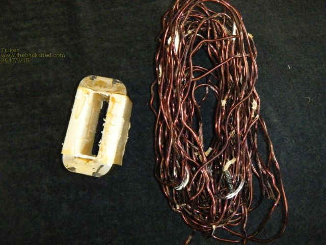
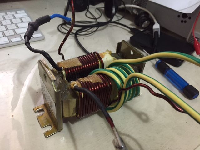
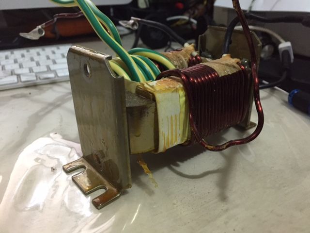
Madness, this inductor is out of a smaller Aerosharp. The 3000W units have a different two part choke I think and it is potted in silicon. Anyway, here it is, I hope this helps.
iron laminated core, 17mm x 25mm rectangular section.
I unwound about 30 turns of one side to leave me with the 13. Winding wire is 3mm diamater (7mm2) copper on the 13T, 6mm2 on the 6T. wronger than a phone book full of wrong phone numbers
Tinker Guru Joined: 07/11/2007 Location: AustraliaPosts: 1904
Posted: 02:28am 15 Mar 2017
Copy link to clipboard
Print this post
That's interesting, I have a few of those very similar from the 3KW aerosharp units.
I might just try to unwind one and see what kind of choke that core makes. Klaus
Madness Guru Joined: 08/10/2011 Location: AustraliaPosts: 2498
Posted: 11:45am 15 Mar 2017
Copy link to clipboard
Print this post
Thanks Poida.There are only 10 types of people in the world: those who understand binary, and those who don't.
Warpspeed Guru Joined: 09/08/2007 Location: AustraliaPosts: 4406
Posted: 01:16pm 15 Mar 2017
Copy link to clipboard
Print this post
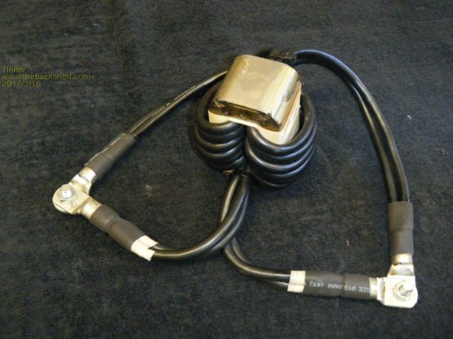
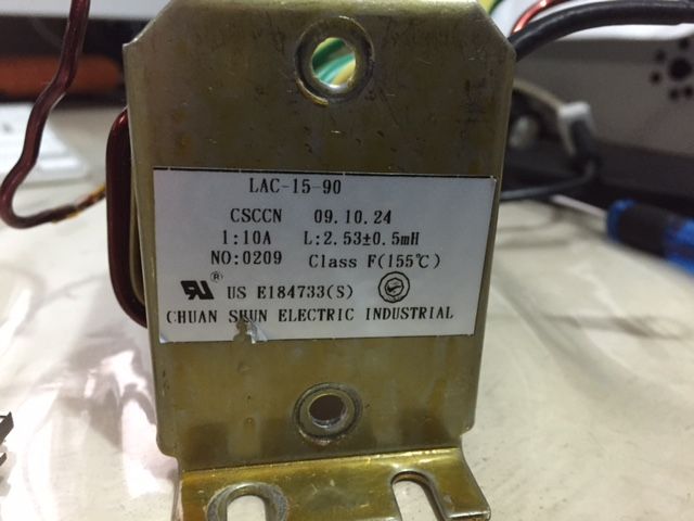
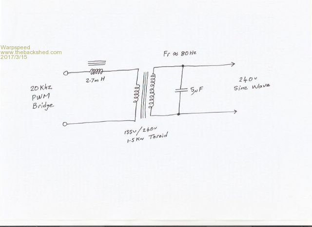
I can tell you all about those chokes, I have several here pulled from 1.5Kw Inspire grid tie inverters. Not identical but almost so.
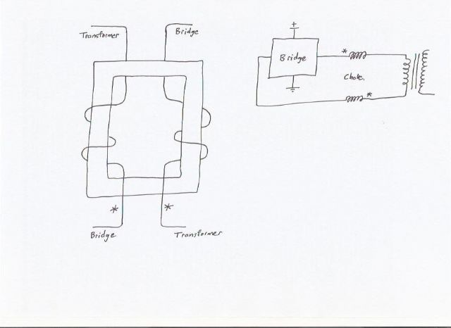
This choke, along with the toroidal transformer, and a 5uF capacitor form a very clever composite filter to turn the PWM into a nice smooth sine wave.
The 5uF capacitor and the transformer secondary form a tuned circuit resonant at roughly 1.5 times 50Hz. The reason it is not tuned to exactly 50Hz, is that would cause a massive uncontrollable build-up of voltage under no load. By tuning it to 1.5 times the frequency, any stored resonant energy in one cycle appears exactly out of phase during the following half cycle.
This 75Hz resonant circuit, particularly the 5uF capacitor will have a rapidly decreasing impedance at frequencies higher than 75 Hz, and will greatly attenuate the 20 Khz PWM and its harmonics.
To assist this, and not shunt the PWM bridge with a very large capacitor, a series choke is fitted that has a low impedance at 50 Hz, but a very high series impedance at 20 Khz.
This combination is an excellent way to turn high frequency PWM into a 50 Hz sine wave with very high attenuation of the higher frequency components.
There is also the hidden advantage that the circulating energy between the transformer secondary and capacitor, even though it is not resonant, reduces the effective magnetising current (as seen by the PWM bridge) and no load loss created by the transformer.
The choke you have is not a common mode choke, although it looks exactly like a common mode choke. The phasing of the windings will be different. Your choke will be a split choke with half the turns on each side, which is a much nicer way to do it than the Inspire choke which is all on only one side of the PWM bridge.
The coke I have here is marked 2.7mH, but it actually measures closer to 3.4mH. The inductance is not that important. I cannot remember what I measured as the saturating current, but it was pretty high, 40 to 50 amps as I recall. So it must have a very large air gap buried in there somewhere. Cheers, �Tony.
greybeard Senior Member Joined: 04/01/2010 Location: AustraliaPosts: 172
Posted: 05:48pm 15 Mar 2017
Copy link to clipboard
Print this post
I keep seeing this thread title and start salivating about home brew beer.
Tinker Guru Joined: 07/11/2007 Location: AustraliaPosts: 1904
Posted: 12:48am 16 Mar 2017
Copy link to clipboard
Print this post
So I grabbed the 3KW Aerosharp choke I had and unwound it. Its quite a job but fortunately the 3mm wire is stiff enough to push it through the slot. The first hurdle is to undo the clamping bolt, the nut only budges after it has been persuaded with a little blow torch .
Then I ended up with this:
900gram of scrap copper wire and a core with an opening of 70 x 16mm.
The choke as it was is is no good for the rather high primary currents I expect on my inverter.
So I rewound it. 20 sq mm cable just fits 16 times into that slot. This gave me me 4 turns of 80mm sq. (4 x 4 in hand)
Now it looks like this:
The rather unorthodox winding style was because the only way I could fit the wire was to push it through from the same side, using no cross overs. As shown its connected for 4 turns but by opening one side it could be 8 turns of 40 mm sq. (2 in hand).
Tomorrow might be a chance to see if it works any different from the ferrite chokes I have been experimenting with so far.
I hope the core is laminated from a continuous strip - I did not remove the insulation to see if it was a split C type core. The laminations are very thin though.Klaus
Warpspeed Guru Joined: 09/08/2007 Location: AustraliaPosts: 4406
Posted: 10:48am 16 Mar 2017
Copy link to clipboard
Print this post
It will be a split C core with a pretty big air gap. This is going to behave very differently to an ungapped ferrite core.
A ferrite core will very quickly saturate at only a very few amps, so its only going to do anything during the very short time interval the mosfets are switching.
This gapped iron choke is going to be a full time inductor,its going to be there all the time with the full inductance.
From memory my Inspire choke had 42 turns on each side (84 turns total) and 3.4mH. If I rewound that with 8 turns total, the inductance would fall to 32uH. The saturation current of the original was somewhere around 45 amps, that will have now increased to maybe 460 amps.
So that 32uH is not going away.
This is going to be very interesting. Just make sure you have the two windings phased correctly so they are in series.
Edited by Warpspeed 2017-03-17Cheers, �Tony.
Tinker Guru Joined: 07/11/2007 Location: AustraliaPosts: 1904
Posted: 11:03pm 16 Mar 2017
Copy link to clipboard
Print this post
It kind of worked, with the windings connected as 8 turns in series and used on one side of the primary. The idling current was higher than either of my ferrite chokes (E-core & ring core).
With a load (I only did up to 600W) there was no squiggle at the zero crossover.
Now I'm getting more cable lugs so I can re connect the 6 turns on my ring ferrite core into 12 turns. From what I learned so far, more turns = lower idling current.
I'm still waiting for the little inductance meter I ordered from e-bay. I should then be able to measure what inductances my choke variations have.
As you mentioned in another thread, building an inverter from scratch is nowhere near as easy as it looks from the schematic. Klaus
Revlac Guru Joined: 31/12/2016 Location: AustraliaPosts: 1151
Posted: 12:37am 25 Mar 2017
Copy link to clipboard
Print this post
Just a quick question? when reducing the value of the gate resistor di/dt is generated when high currents are switched too fast. This is due to stray inductance present in the circuit, which produces a high voltage spike (Ringing) and sometimes death to the fets. since most of us build our own H-BRIDGE the inductance will vary a bit. So i think the gate resistor should be sized to suit each different build or at least adjusted sacrificing some efficiency for reliability.
Deciding the value of the pull-down resistor? Usually the purpose of a pull-down is to keep the FET off during startup,
the value of gate to source resistor most inverters i have seen(i haven't seen that many) were 2k-7k resistance.
Now if I'm barking up the wrong tree let me know.
Cheers AaronCheers Aaron Off The Grid
Tinker Guru Joined: 07/11/2007 Location: AustraliaPosts: 1904
Posted: 03:47am 25 Mar 2017
Copy link to clipboard
Print this post
Hi Aaron, I did manage to blow expensive block Mosfets with very little load, hence relatively small switching current.
The pull down resistor was 10kOhm, same size as on the EG002 board.
It may take a while but we try to get to the bottom of these failures.
I have now a little inductance meter (cheap on Ebay) so I can measure what inductances there are in play.Klaus
Madness Guru Joined: 08/10/2011 Location: AustraliaPosts: 2498
Posted: 01:04pm 25 Mar 2017
Copy link to clipboard
Print this post
Gate source resistors need to keep the gate off when it is supposed to be off. Perhaps 20K that we are using is too high, easy enough to try, I can put another 20k in parallel and see if that has any effect on a board I have that works but is producing spikes so I have only run it for a few seconds at a time, that will make it 10K. With 6 FETs this may behave differently than 1 big FET with only 1 gate.
From how I see it the things that will kill FETs is over current which could happen if both sides of the bridge happen to turn on at the same time. Working them hard when the inverter is running properly does not seem to cause any issue if they are kept at a reasonable temperature. Over temperature would kill them also but I have never measured more than 60 degrees with the big heatsinks I am using. Even running at 8KW for over 30 minutes with ambient temperature over 35 degrees. The other big killer is over voltage, this could come from snubbers not doing their job properly.
Edited by Madness 2017-03-26There are only 10 types of people in the world: those who understand binary, and those who don't.
Warpspeed Guru Joined: 09/08/2007 Location: AustraliaPosts: 4406
Posted: 02:06pm 25 Mar 2017
Copy link to clipboard
Print this post
Spot on there Aaron.
Power up and power down are absolutely critical periods. This is more usually a problem with higher drain voltage mosfet applications. But really large low voltage devices can have pretty high internal gate to drain capacitance which can be a problem. Agree, 2K to around 10K seem to be popular. Any half decent gate driver should be able to handle a few hundred ohms without breaking into a sweat.
If you are as paranoid as I am about all this, a 15v to 20v zener diode between gate and source plus the resistor will provide some additional protection at little cost.
There are really two very different problems here. Spurious turn on can cause cross conduction and uncontrolled current flow. Or just the voltage spike on the gate can break down the gate oxide and destroy the device without the huge current.
I am now convinced we are being flooded with cheap Chinese fake parts that fall way below data sheet specification. So there may not be a problem with your circuit, but the device itself could be junk. Edited by Warpspeed 2017-03-27Cheers, �Tony.
Madness Guru Joined: 08/10/2011 Location: AustraliaPosts: 2498
Posted: 03:25pm 25 Mar 2017
Copy link to clipboard
Print this post
Changing the resistance had no effect for me, Chinese parts could be a big factor. I will be investigating ways to test MOSFETs, one thing I will be doing is stress testing them in groups of 4 on the mini inverter I made recently.There are only 10 types of people in the world: those who understand binary, and those who don't.
Warpspeed Guru Joined: 09/08/2007 Location: AustraliaPosts: 4406
Posted: 03:47pm 25 Mar 2017
Copy link to clipboard
Print this post
I am going to start measuring Rds on, as well as testing gate and drain breakdown voltages. The Chinese integrated circuits seem to be o/k, but I am seeing more and more problems with power devices being sub standard.Cheers, �Tony.
Madness Guru Joined: 08/10/2011 Location: AustraliaPosts: 2498
Posted: 04:26pm 25 Mar 2017
Copy link to clipboard
Print this post
I have been measuring RDS on but not others, I would be interested if you could post any info on how to do that.
I recently had a power board that I tested after adding 1 MOSFET to each of the 4 legs, while doing this I had no capacitors on the pcb. It worked perfectly with very low idle current and perfect waves right through to and including having all 24 MOSFETs on board. Then I added capacitors and the whole thing went pear shaped. Idle current went from >15W to around 250W and lots of spikes in the waveform. Only change was adding capacitors, I may be wrong but I suspect both sides of the bridge are on for a few nanoseconds. While there were no caps on the PCB it could not draw much current.There are only 10 types of people in the world: those who understand binary, and those who don't.
Warpspeed Guru Joined: 09/08/2007 Location: AustraliaPosts: 4406
Posted: 07:26pm 25 Mar 2017
Copy link to clipboard
Print this post
That sounds plausible.
I have a Danbridge non destructive insulation tester which can test anything for leakage up to 12Kv. But without that, all you can really do, is just short the gate to source and put some dc volts across the drain to source, with a high value current limiting resistor. If it breaks down, you know it was a dud.
Pretty much the same with the gate. Test it up to about 20v and see if it survives.
You might trash a few devices that way, but that is better than having one sub standard mosfet blow up multiple other good ones.Cheers, �Tony.
Madness Guru Joined: 08/10/2011 Location: AustraliaPosts: 2498
Posted: 09:52pm 25 Mar 2017
Copy link to clipboard
Print this post
I have a 1KV insulation tester, is that sufficient?There are only 10 types of people in the world: those who understand binary, and those who don't.
Tinker Guru Joined: 07/11/2007 Location: AustraliaPosts: 1904
Posted: 10:14pm 25 Mar 2017
Copy link to clipboard
Print this post
Gary, your comment about adding capacitors caused the mosfets fail is strange. Perhaps your capacitors are suspect?
While I was testing with my 4 mosfet rig and a 3 speed desk fan on full power as load, I could observe little spikes near the crossover point. Adding a 10,000uF capacitor completely removed those spikes.
Another thought, on the EG002 schematic they show interlocking transistors between the 8010 and gate drivers. They put them there for a reason I assume. Worthwhile to test this?
Everything is on hold here, still waiting for toner transfer paper so I can make a different PCB for my inverter mosfets.Klaus
Madness Guru Joined: 08/10/2011 Location: AustraliaPosts: 2498
Posted: 10:47pm 25 Mar 2017
Copy link to clipboard
Print this post
Why don't you try the method I put up using the oven for 5 minutes, no toner transfer paper required and works very near 100% perfect. I have polished it with a cloth after etching and apart from scratching or using acetone the toner will not move and it is completely impervious and the end result is very near perfect.
The MOSFETs did not fail but it had spikes in the waveform and idle current went through the roof. I only ran it for a few seconds like that and shut it down. How the caps could cause the fault is a mystery to me as far as I know all they did was make more current available. Before turning on the inverter there was no current flowing.
I have the same circuit on a reduced size board with just 8 MOSFETs in total and 4 of the same capacitors and it runs like a dream.Edited by Madness 2017-03-27There are only 10 types of people in the world: those who understand binary, and those who don't.
Tinker Guru Joined: 07/11/2007 Location: AustraliaPosts: 1904
Posted: 12:57am 26 Mar 2017
Copy link to clipboard
Print this post
Hi Gary, You know the saying about old dogs and new tricks?
Anyway, I re read what you wrote:
"I print out the images on glossy paper with a laser printer and put the printed sides inwards, carefully line them up with a bright light behind and staple them together. Cut the PCB to size without touching it with your bare hands at any stage prior to heating, scratch up the surface with 180 grit sandpaper and then clean with acetone. Once dry (wet acetone will dissolve the toner) put the PCB between the sheets of paper and run through a preheated laminator at full temperature several times. Then I put the PCB in the oven at 180 for 5 minutes while the laminator is on. Take it out of the oven and straight through the laminator a couple more times. I know of at least one person who has done this with an iron rather than the laminator. The baking in the oven is important to get a nonporous layer of toner."
Question 1, what kind of glossy paper? I do not have any.
Question 2, when you say "take it out of the oven and straight through the laminator a couple more times", would that not ruin the image by scrubbing from the hot rollers? Or do you have the board between to clean sheets of white paper then?
BTW, I clean my boards with the fine ss scrubbing pads, the soapy ones, under running water. They come out very clean and no copper gets sanded off. Then spray with PCB cleaner and wipe off any pad residue with a paper towel.
I am weary to use acetone after the etching to get the toner off, always did that with the ss pads as well. Klaus
Page 2 of 48
Print this page
The Back Shed's forum code is written, and hosted, in Australia.


 .
.