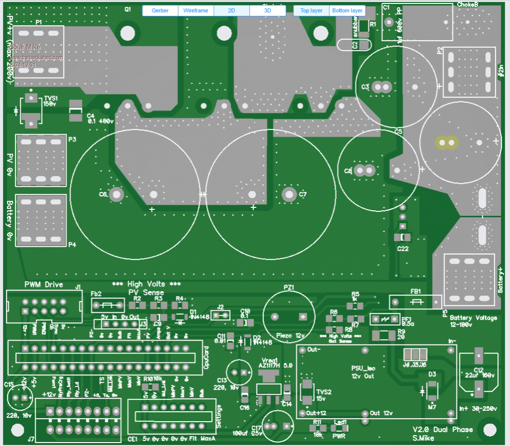
Another project for the new year, we have had our MG EV coming up to 2 years now, so I have decided to charge it during the day from a bunch of PV panels mounted on posts above the drive leading down to the garage under the house. The car will drive under the PV array to get to the garage. The drive is 3m wide, this will allow 3 series panels across and 3 bays, 9 panels in all. I have purchased 440W Bifacial panels as they are on sale for $134 each, with free shipping, panels have arrived, waiting on rails and other mounting clamps etc.
The plan is to build a small shed next to the array to house the PV charge controllers and a small 3kw HF inverter, plus 16 200AH CALB Lifepo4 cells that are currently unused gathering dust. The EV's 2KW granny charger will be used to connect to the inverter and thus charge the car via the PV array and 48V battery bank. The battery will act as a buffer if the sun isn't strong enough, otherwise the HV relay in the car will switch off and on with voltage drop-outs.
I'm a great believer in using multiple smaller charge controllers rather than a single monster design, so for this application I will use 3 small Diy charge controllers each connected to 3 series panels for 1300 watts.
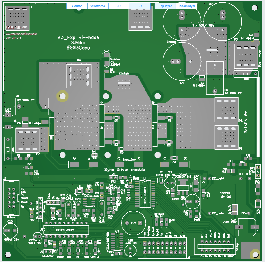
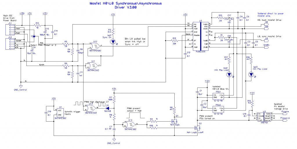
I have been playing around with a smaller design in the last month or so, using synchronous buck conversion and dual phase output. The first version used bootstrap circuitry to power the H0 buck stage, great fun getting that working ok, there is a very fine line for the synchronous mosfet rectifier at low duty cycles to start acting as a reverse boost converter, software has to continuously test to see what the charge current is, as it can no -ve and blow things up; finally managed to destroy 3 mosfets and a couple of driver chips in getting it to work reliably.
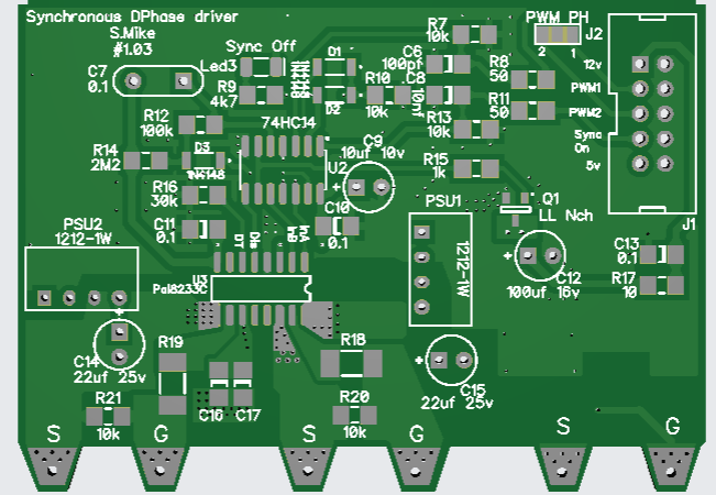
Slight redesign of the driver board using 1 watt isolated 12-12v PSU's for the H0,L0 bias supplies, making things much more reliable, as now the synchronous rectifier mosfet stage can be turned off at low charge currents automatically using a comparator, this puts it into asynchronous mode using its internal drain-source diode, thus preventing boost mode operation from destroying things.
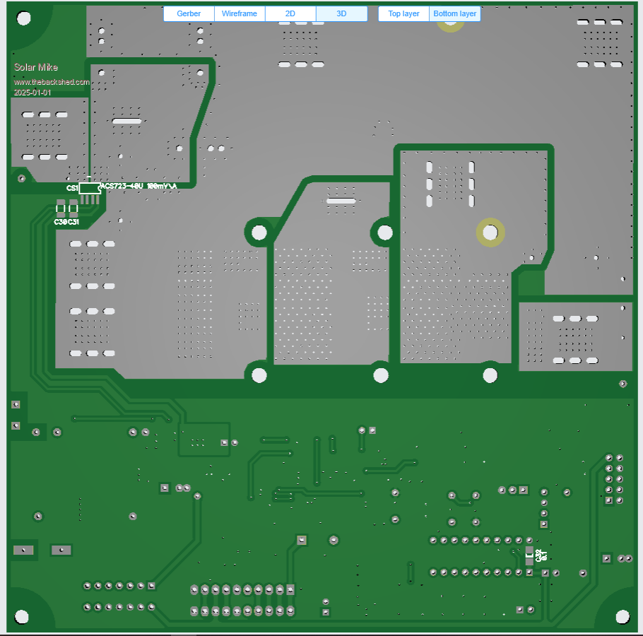
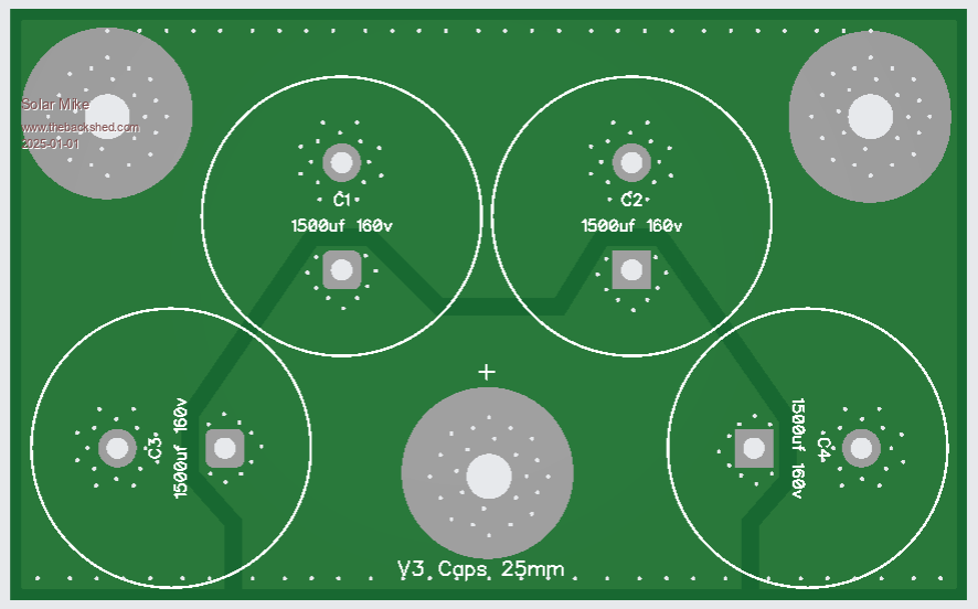
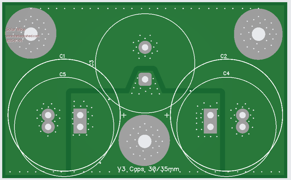
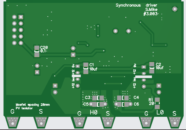
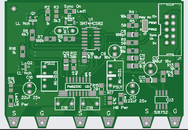
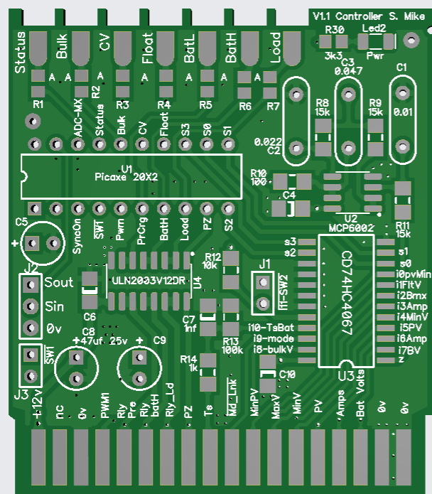
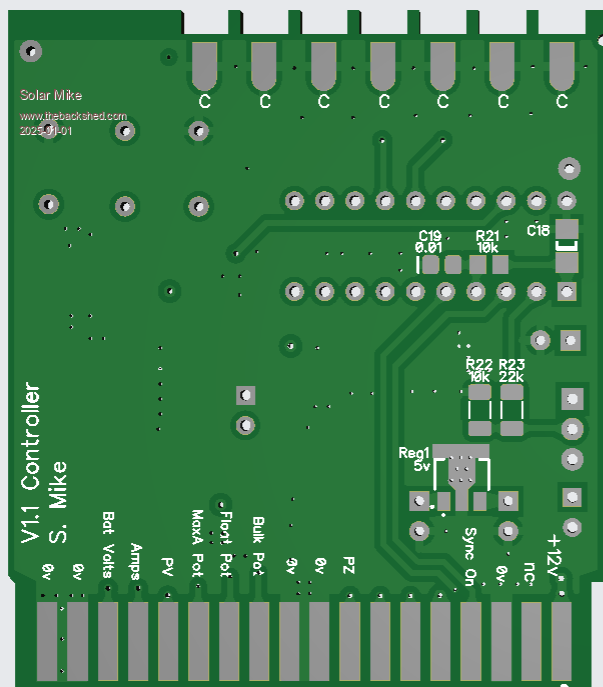
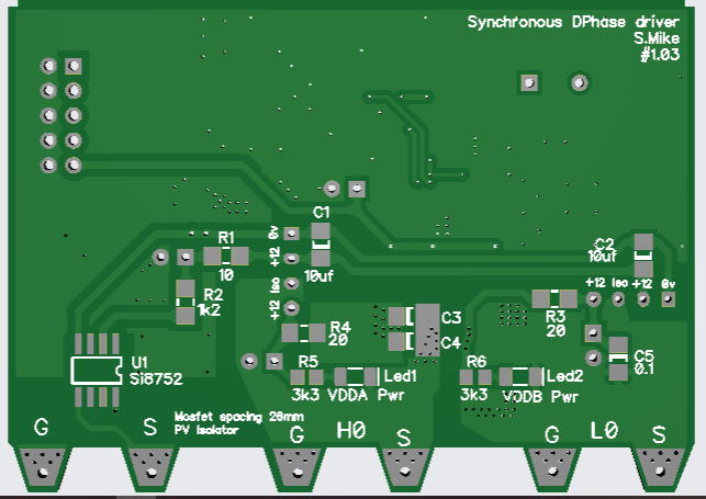
Here are some of the PCB designs: 150 x 150mm
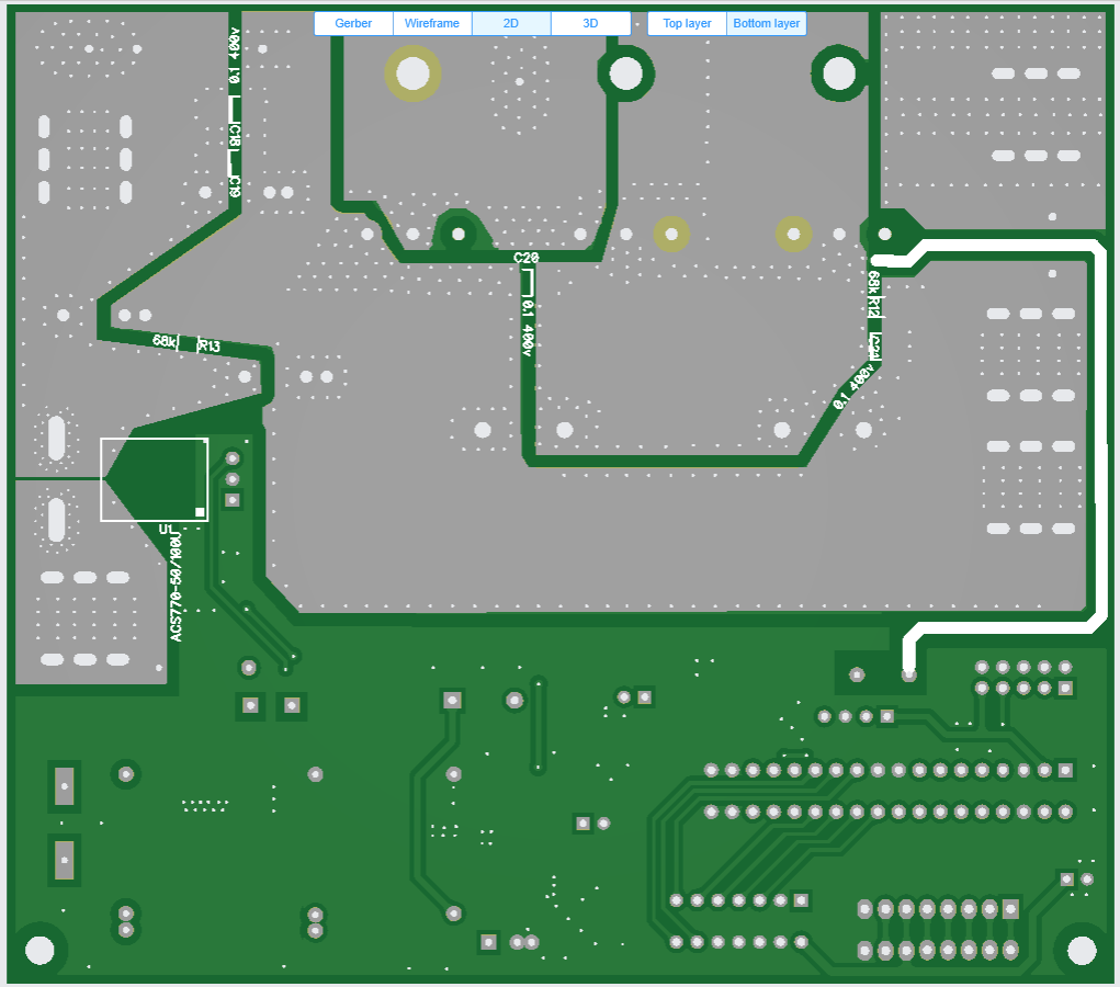
The main mosfets are TO-247 200v types (DWX9R820H from LCSC) bolted under the pcb to the alloy case, I originally had 150v rated ones and occasionally one would self destruct when running off a 120v DC supply, caused by a 100Mhz 20V ringing spike, a 2200pf cap and series 6R resistor snubber across the L0 synchronous mosfet cured that issue.
CPU is a Picaxe 20X2 on a small 4 layer pcb that plugs into an edge card socket, the other edge card socket has the setting up pots on a small pcb, when unplugged their values are stored in the cpu's eeprom memory.
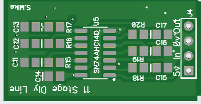
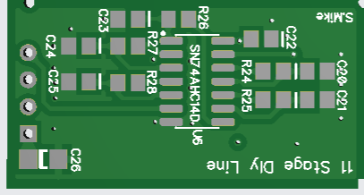
A small pcb module has an 11 stage RC digital delay line for generating the 180 degree other PWM drive phase, the ribbon cable going to the mosfet driver pcb can be extended to another main board power stage (no cpu or associated bits) to increase the power handling if required.
Charge state leds are soldered along the top, an analog mux is used to sample data inputs, its output via an active filter to the cpu's ADC input.
CPU Card (4 layer)
The mosfet driver pcb sits directly on top of the main mosfet pins, using some logic gates and a Pai8233C-S1R isolated half bridge driver chip; this keeps all current drive loops short and allows for an easier pcb design of the main buck circuitry. When pwm drive is turned off, the driver chip and the 2 psu's are shut down to save power.
Driver Card:
Phase generator Card:
Cheers
Mike
Edited 2025-01-01 06:23 by Solar Mike