| Menu | JAQForum Ver 19.10.27 |
| Menu | JAQForum Ver 19.10.27 |
Forum Index : Microcontroller and PC projects : DIP2350
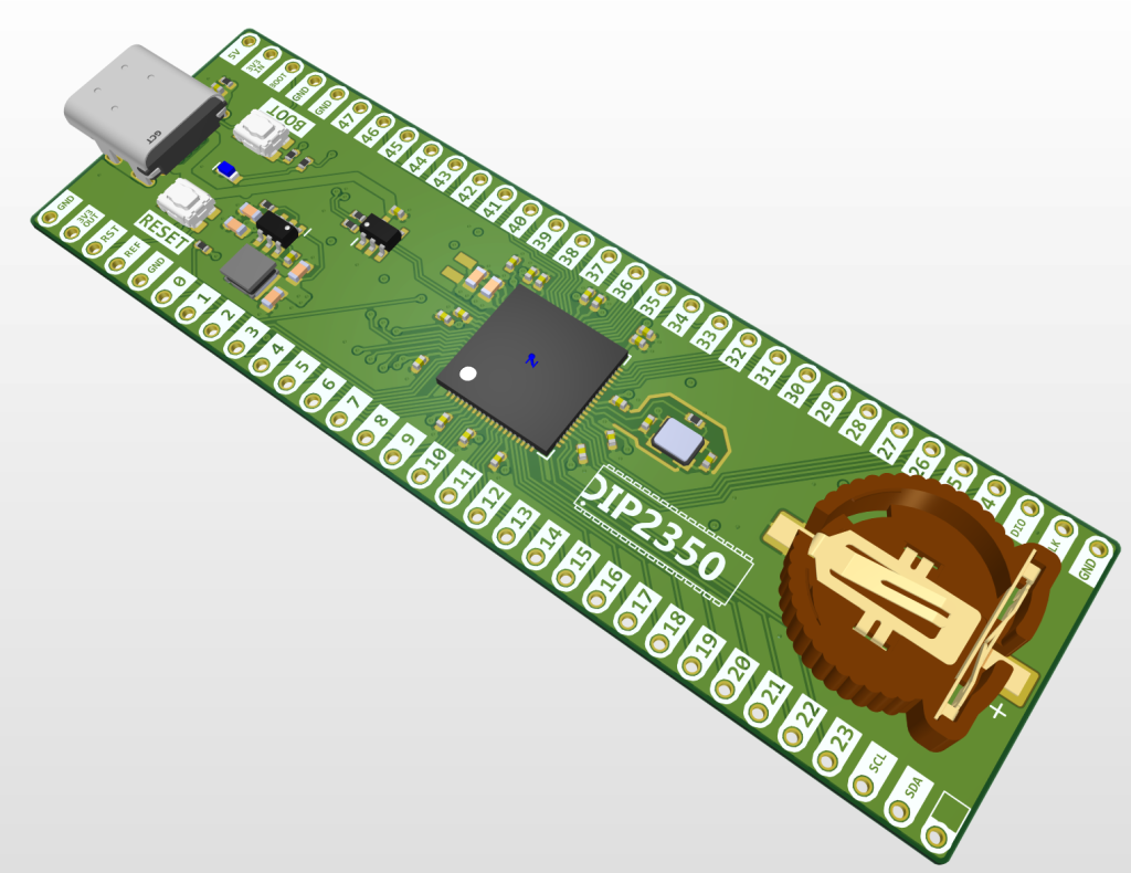
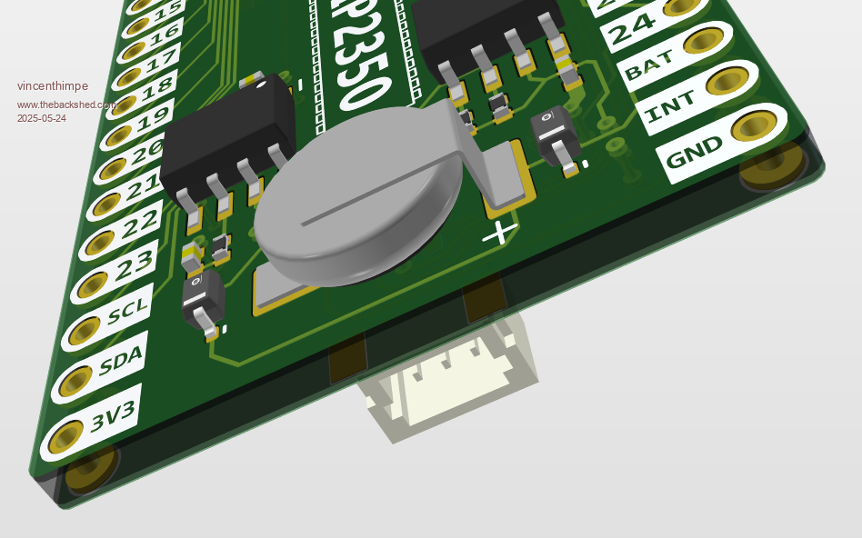
GIThub Link An RP2350 Packaged as a 64 pin DIP package. This can run MMBasic or CircuitPython or anything you want. The intended use is as a MICROCONTROLLER in an EMBEDDED application, not as a computer. Think STM32, PIC32 kind of application. Using a standard DIP64 allows simple thru-hole construction , breadboarding etc. it fits a standard 64 pin socket. No need for castellation or weird pin spacings - USB Type-C connector. Right angle , thru hole for mechanical stability. Long overhang so you can have this go through an enclosure wall. - USB powered or self powered. Self powered up to 12 volt. - Ideal diode / or-ing / e-fuse circuit (optional) to prevent backfeeding usb. - Current limit on the ideal diode. The circuit can be used as a power or-ing to provide backup power from a Li-Ion cell and charger - ESD protection on the USB port using TVS diodes - 3v3 DC/Dc regulator can deliver up to 1A of load current. In this case you need to provide 5v as USB cannot provide source current. - RP2350B in 80 pin QFN with all 48 GPIO brought out. - Flash 128Mbit - optional PSRAM on GPIO47 - optional 3v reference for analog circuitry LM4040-3 - Heartbeat led on gp25 with solder bridge. Can be removed from circuit. - Using Abracon XTAL and polarized inductor for 1v1 regulator - Boot and Reset button. Secondary boot button under usb so you can use a paperclip through the enclosure to force boot. - on board, optional i2c bus : I2C EEPROM or FRAM I2C RTC with battery backup 1220 cell. - cheap version using an M41t11 - precision using a MEMS DS3231. Option to use brown-out detection to hold cpu in reset till power stabilizes. Optional interrupt on GPIO21. User needs to wire the i2c bus to desired io port. - 4 layer board with controlled impedance and power planes. Board designed so it can be made at OshPark, JLCPCB or PCBway - CAD source available under Creative Commons ZERO . Public Domain License. Altium Format. - Production pack (gerber/drill/bom available. - BOM is procurable from Digikey/Mouser as well as LCSC (Asia) with direct LCSC order codes if you want this to be partially assembled by JLCPCB. - Pinheaders to be used are the turned pin type. Not the square Dupont style that destroys breadboards and ic sockets. Preci-Dip or equivalent. Comments welcome |
||||||
But no photo of one. I wonder if it works? Peter's does. |
||||||
|
||||||
|
||||||
photos uploaded. PDF too. but there's more on Github. I'm ordering first boards this weekend. still doing some tweaks. I'm not happy with the battery. the SMD mountable batteries and supercaps seem to be disappearing. |
||||||
Thank You for sharing your design. Fair warning, the QSPI buss to the flash and PSRAM are high speed signals! Use good routing practices as you would with radio frequency signals: Short traces, no 90 degree bends and vias are likely problematic. Most of the successful "reference" designs have the flash and PSRAM on the same side of the PCB as the RP2350 to avoid issues with the high speed QSPI signals. |
||||||
Understood. QSPI is length matched to within 20pS from each other. Which is more than an order of magnitude above what is allowed. |
||||||
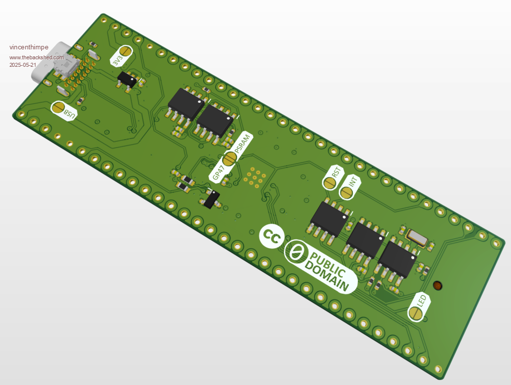
RC2 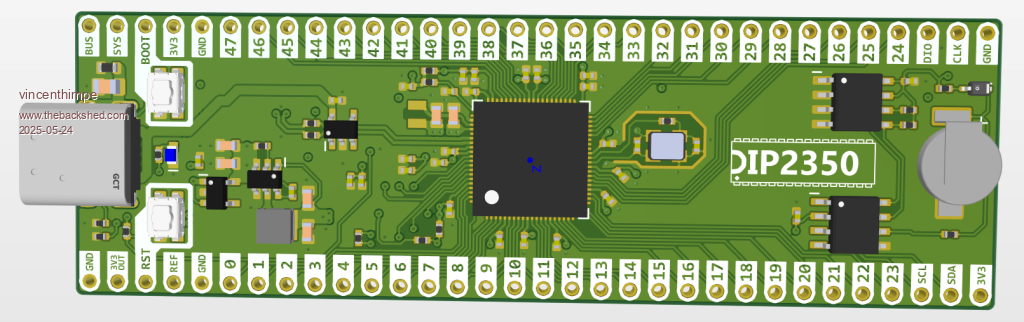 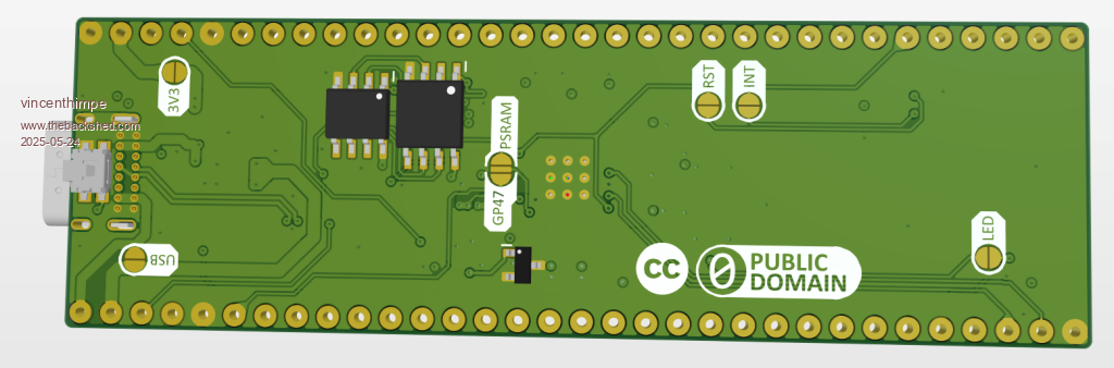 Changes - Moved all parts (except flash, psram and reference diode to top. This reduces cost at JLCPB for assembly. - Length tuned QSPI to within 50pS (as per QSPI spec) - replaced the 1220 cell + holder by a rechargeable cell. - added charging circuitry for the new cell - removed cheapo RTC option. The BOM cost is equal to the DS3231M. Makes no sense - Added "ideal diode" or-ing controller with efuse (Torex XC8110) . This blocks reverse feeding USB. This device is also an "ideal diode" with less than 80mV drop. - Brought out USB power before OR-ing controller. This allows to use USB as supply for a LiIon charger and backfeed the Battery voltage into Vsys using a second OR-ing controller. - cosmetic changes to labeling - changed from 24C128 to a 24F64 FRAM by default in the BOM. - fixed a mistake with the 3V reference diode. It was clamping the wrong power pin. - changed the 0603 resistors to 0402. - layer stackup confirmed with JLCPCB and impedance tuning on USB modified accordingly. The only parts on the bottom are : The PSRAM and Flash. To be installed by user. PSRAM is optional and hard to get. The 3V reference diode (LM4040-3) for the ADC. This is optional. The changes allows JLCPB do the assembly as a single sided (top only). User needs to install flash and USB connector to avoid "handsoldering fee" The USB connector is completely thru-hole for mechanical strength |
||||||
hi Vincent, i'd strongly suggest dropping the onboard battery, it will almost certainly leak at some future time and cause users heartache. far safer to provide a small 2-pin connector for plugging in a battery, or even better bring it out on one of the side pins. could DIO and CLK be moved to a debug connector to free up side pins? also, if possible sticking with 0603 or larger parts will yield a far more mechanically 'robust' assembly. cheers, rob :-) |
||||||
Sealed lithium cell ( not lithium ion ) . They don't leak. Same cell used in solar watches. it's actually more of a supercapacitor than anything else. Charging is sub milliampere. Having an external connector is a good idea. you can hook up an external 3v coin cell in a holder.. i'll use a JST style connector. 0603 is not possible. It needs to be 0402 due to the placement requirements. The only 0603 are the tank capacitors for the switcher and that's simply because i need to be able to route between the pins to get to the inductor. There it makes sense. The build is optimized for cost of assembly and BOM. The only thing the user needs to install is the USB connector and the flash. You can ask JLCPCB to do the USB connector it but it is a manual work and they ding 5$ for that. The flash is a backside pick and place and that pumps up the price again. Since different applications may require different flash sizes, this is left to the user. Same for the FRAM. Not everyone needs that. Design/cost of assembly/bomcost trade offs. The design idea is a basic programmable microcontroller. It's not intended to be used with VGA or HDMI output, or play videogames. It's an embedded controller that sits in a box somewhere doing its thing. Think test equipment, or some black box that has no, or minimal user interface. STM32 , 8051, pic18 , pic32 kind of stuff. But with the flexibility of on-board basic. No mucking about with endless compile , fix bug, recompile, fix typo, recompile , reflash cycles. All GPIO is brought out without restrictions. If you want to use the PSRAM it attaches to GPIO47. I want to retain the ability send out 32 bit in a single cycle on the GPIO. Using GPIO0 for PSRAM requires bit shifting and doing two cycles to shift bit 31 onto the higher port. (it is not possible to do 64 bit operations. The AMBA bus is 32 bit only, so you need two cycles. I deliberately did not lock-in things like SDcards cause it requires sacrificing I/O. Simply install a large Flash and use the file system there. The i2c subsystem is not wired on purpose. In many applications you don't need the RTC or FRAM. I could push the SWDIO and SWCLK onto a JST connector. and reclaim two pins. It would allow bringing out the Int pin of the RTC and feed VBAT.... i need to think about that. That may be worth doing. I'm never going to use that debug port, and it would open the pins for external battery if you don't want it on-board. Good suggestions ! thanks ! |
||||||
 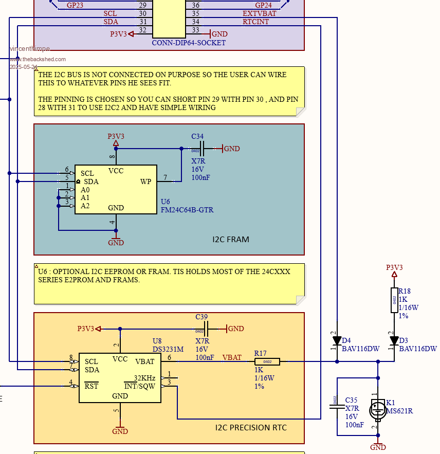 changes implemented - added JST debug connector - freed up the SWDio and SWCLK pin - brought out EXTVBAT so you can power this from an external call ( like the main power cell ). Note : user is responsible to regulate this to 3.3 volt ! you can't hook up a LiIon raw cell voltage. There is a backfeed protection with a low-leakage diode. - moved RTC INT to its own connector pin so you are no longer locked the GPIO21 but can wire this where-ever. |
||||||
Assuming that R18 is intended to limit the charge current into the battery, wouldn't it be better moved so that the D3/D4 form a wired OR from EXTVBAT and P3V3 then R18 to the battery and R17 off the junction of R18 and battery pos? That way the battery has protection against someone putting 3V3 or even 5V on the EXTVBAT pin. A dual diode might save you some PCB space too as EXTVBAT and P3v3 aren't far apart on the connector so it's only a single trace from the diode package to R18 then the battery. |
||||||
i thought about the dual diode but the BAV170 is typically a SOT23. The smaller version (sot 323 or 523) is only made by one manufacturer, and lcsc doesn't have it, or very limited. Those diodes need to be very low leakage. The cell is very small capacity (3mAh with a max allowed discharge current of 10uA. The current draw from vbat is around 3.5 microamps. The BAV17x leakage ( reverse) is in the order of 5pA. just spotted a mistake :i need to change the value of R18. the charge current would be to high for the little cell. max 100uA. so i need 30k or more. R17 is a current limiter for the RTC. if that device has a catastrophical failure it won't short the cells R18 is a charge limiter for the on-board cell (if installed) There's 2 use scenarios : 1) Self powered or usb powered device WITHOUT on-board battery. - install the on-board cell and done. the cell will be charged when the device is powered. - don't install on-board cell but hook up a 3v non-rechargeable coin (think CR2032 and likes) cell to BAT pin. D4 blocks any reverse current to a non-rechargeable cell 2) battery powered device - install on-board rechargeable cell and done. - don't install on-board but feed 3.3 volt into BAT. User is responsible how that is made from the system battery. if external BAT voltage is used there is no on-board cell. I's either an external cell , or the internal cell. not both. NO need to depopulate or populate parts. no BOM change. install everything. ( except the cell) |
||||||
| The Back Shed's forum code is written, and hosted, in Australia. |