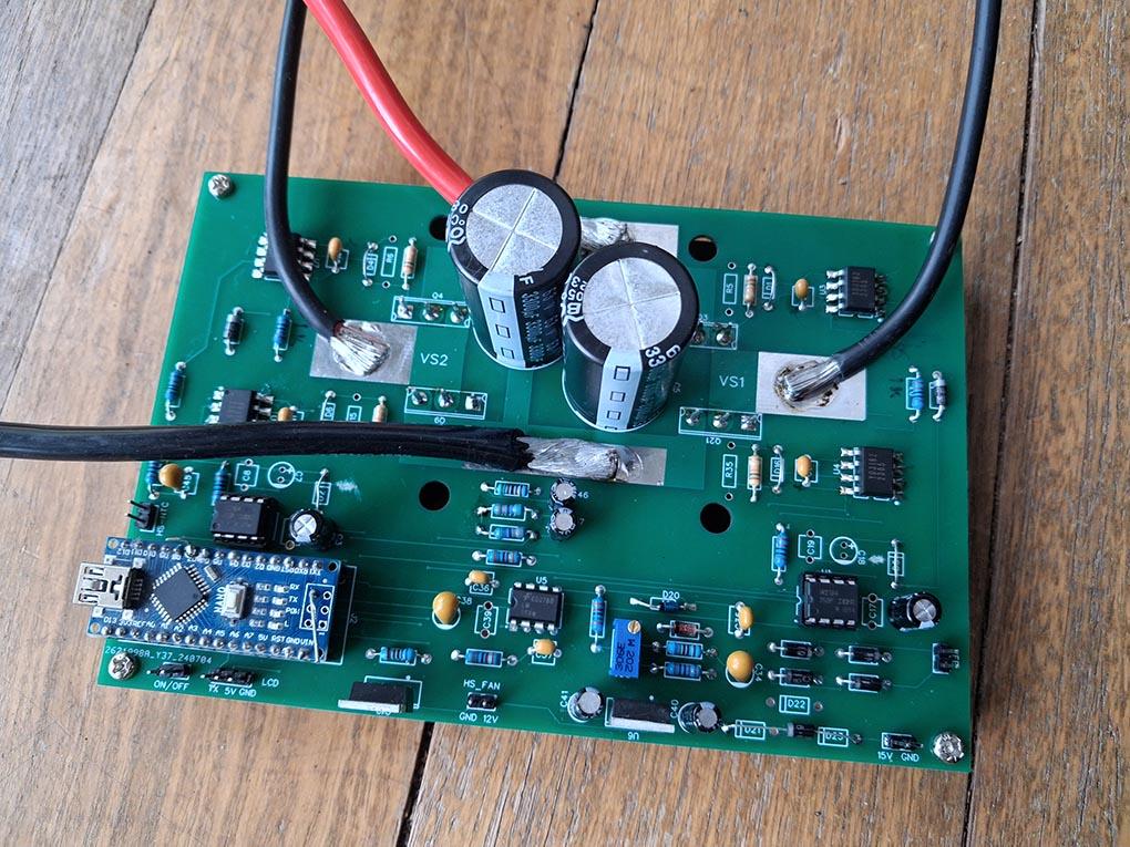
3 15V -> 5V linear reg some 0.1" pin headers 2 heat sink fan FET and gate pull down resistor
I use HY5608 FETs and when fed 50V, only need to switch about 40A so I think these FETs will be just fine.
idle current was 0.2A DC at 54V input for 239V AC output. The toroid makes a huge difference in idle power and I am running this one well below any hint of saturation.
I'm really quite happy with it. Obviously I could build it with thicker V1 and V2 output cables but I just could not be arsed, really.
It runs the picoverter code, which features low DC voltage shutdown with auto restart, fan control for the heat sink and heat sink over temp shutdown.
The semiconductors are: HY5608 80V 360A 1.5 mOhm Rds(on) IR2186 gate drive IC FOD3182 gate drive IC LM358 dual opamp LM7805 linear reg any old logic level FET to drive the fan
it worked first time I applied power!
Edited 2026-01-25 15:50 by poidawronger than a phone book full of wrong phone numbers
Posted: 02:56am 27 Jan 2026 Copy link to clipboard
poida Guru
it works well, only tested it to 1330W AC so far.
for the 1330W AC output (0.99 power factor), input is 54.7V at 29.1A 1590W in, 1330W out, it's 83.5 % efficient
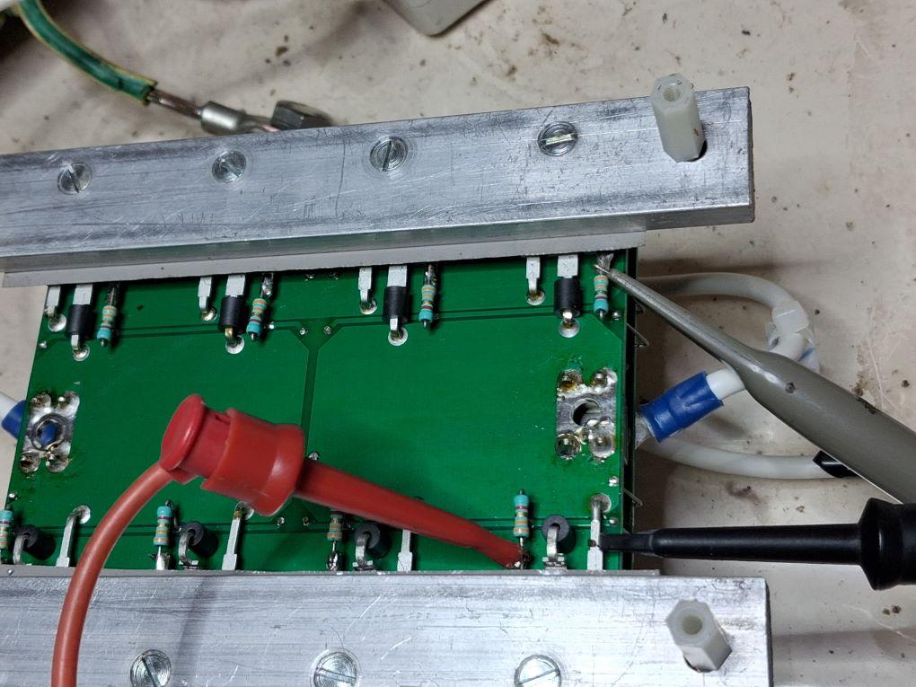
Rather thin wire is used in the primary circuit, it's 4mm2 I think. this wire is the primary winding and I need 3 meters of it. I probably could pick up a few more % if thick stuff was used. the DC resistance of the primary is 48 mOhm. (I determined that by putting 5.8A DC through it and reading 281mV across it)
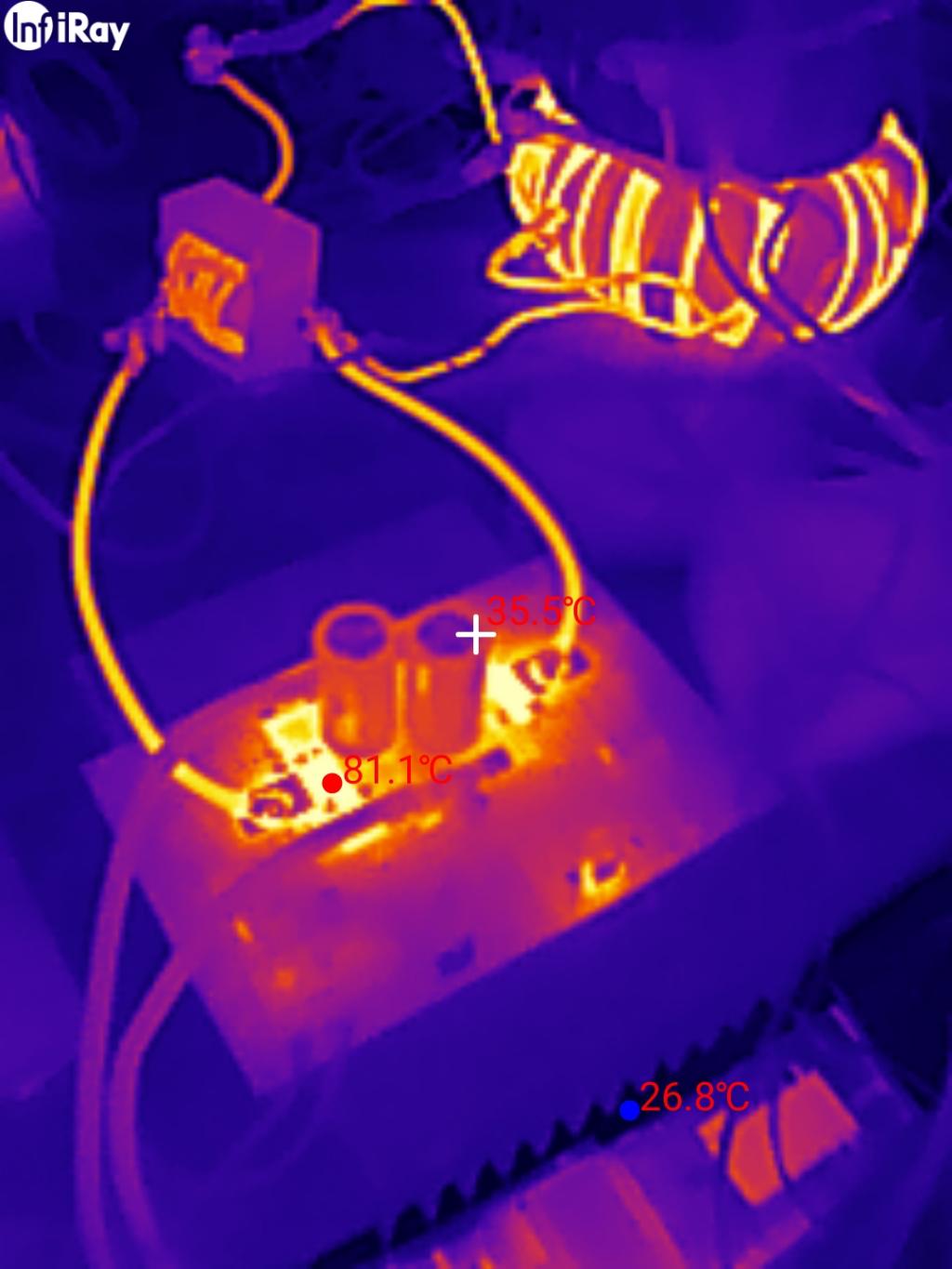
here is a thermal image of it running under this load.
the hottest part is where the low and high side FETs are soldered sort of where "VS1" and "VS2" are located in the above image.
Posted: 06:57pm 27 Jan 2026 Copy link to clipboard
analog8484 Senior Member
Nice little board. Is it 1 oz copper?
Also, curious if you have observed false MOSFET gate turn-on transients like the ones in your past reports on larger inverters.
Posted: 12:23am 30 Jan 2026 Copy link to clipboard
poida Guru
it is 1oz copper, if it shows promise I will make a v.2 with 2 oz copper, error fixes, unused footprints removed and space for 3rd main cap.
I have 3 similar inverters to compare. this one, the first version of it that uses TIP41/42 transistors in the totem pole type gate drive and Wiseguy's inverter with it's professional design.
All 3 require about 1330 W input to drive the same load. Maybe Wiseguy's inverter used 1300 W but the load varies over time so it's hard to get it accurate.
The next thing to examine is gate drive signal shapes and look for shoot through at idle and under load.
I want also to play with more or less capacitor powering the drive side of the FOD3182 chips. At the moment it is only 1uf ceramic with ESR of about 3 Ohms. In the past I have used 10uf electro (ESR of 10 Ohms) with a 0.1uF ceramic parallel.
I varied gate drive voltage while running under load and changing from 12 to 15V made no difference to input power.
Finally, I might need to put "some" resistance in the gate drive, at the moment the FET gate is direct connected to FOD3182 output and I suspect there is MHz oscillation. No doubt that is causing some shoot through.
Posted: 12:26am 31 Jan 2026 Copy link to clipboard
Godoh Guru
That project looks pretty good, Is it going to be usable or programmable for 24 volt as well? Nice looking board, I like the fact that most components are through hole ones. That makes it much easier for us fossils to solder Pete
Posted: 10:46am 31 Jan 2026 Copy link to clipboard
poida Guru
for sure it can be working for 24V. it's always about the current so I would expect only 1kW from it at 24V
I am just seeing if this thing is useful and it's early days.
Posted: 05:35pm 01 Feb 2026 Copy link to clipboard
analog8484 Senior Member
Cool. Look forward to your findings.
Not surprised since the gate caps are fully charged by 10V according to the datasheets. I have tested some HYxxx MOSFETs at 10V and 12V and didn't see any significant difference.
That's a bit surprising. Besides shoot through, the RFI/EMI can be pretty bad as well without any external gate resistance.
Posted: 01:21am 09 Feb 2026 Copy link to clipboard
poida Guru
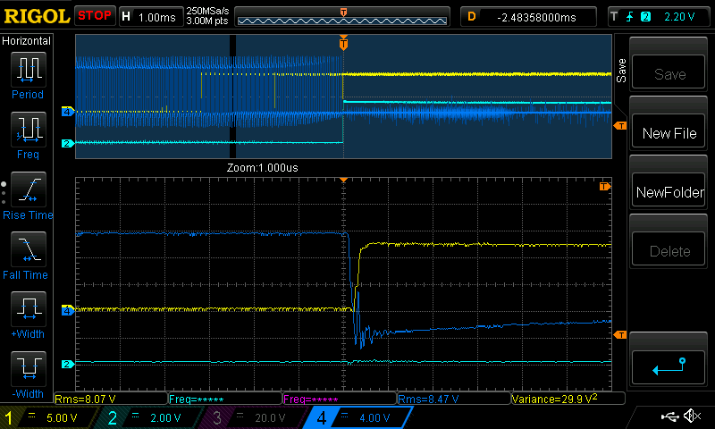
time to look at Gate voltages.
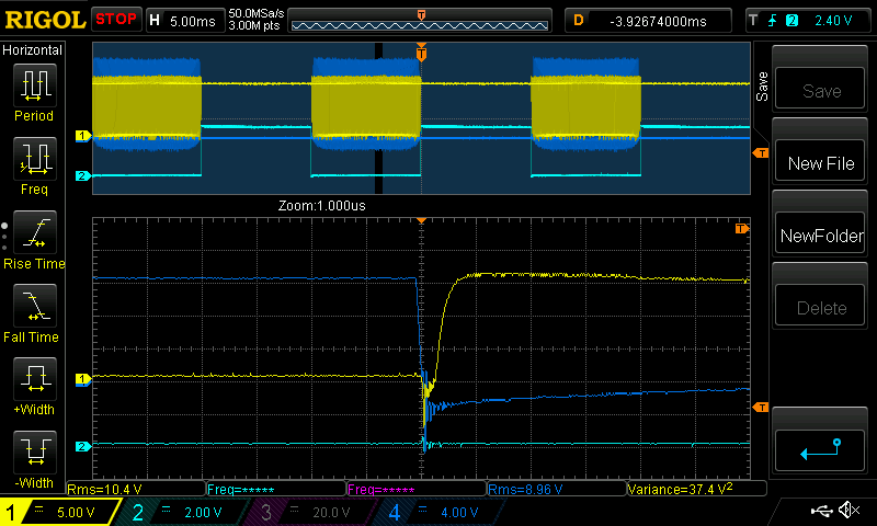
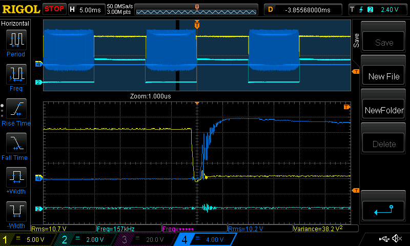
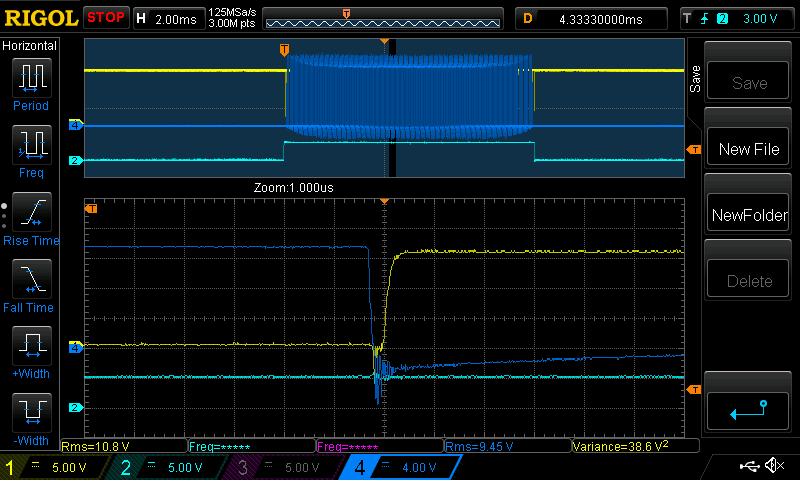
first is the switch on/off for the totem pole board, using a 10R current limit resistor and a 1N4148 diode for faster gate control when pulling it to ground (or source pin) The drive current is supplied by a pair of TIP41 and TIP42 transistors.
test conditions are identical for both boards. 54V DC in, 200W out. Yellow is low side gate voltage Dark Blue is high side gate voltage
and
this is not too bad, not a lot of high frequency ringing.
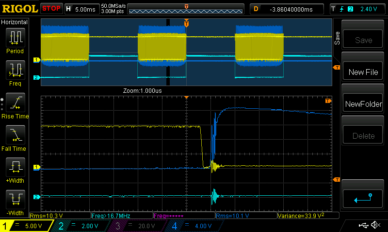
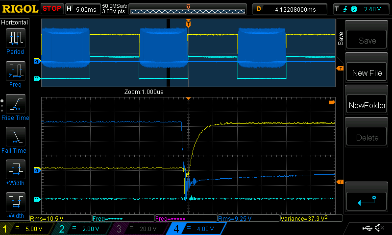
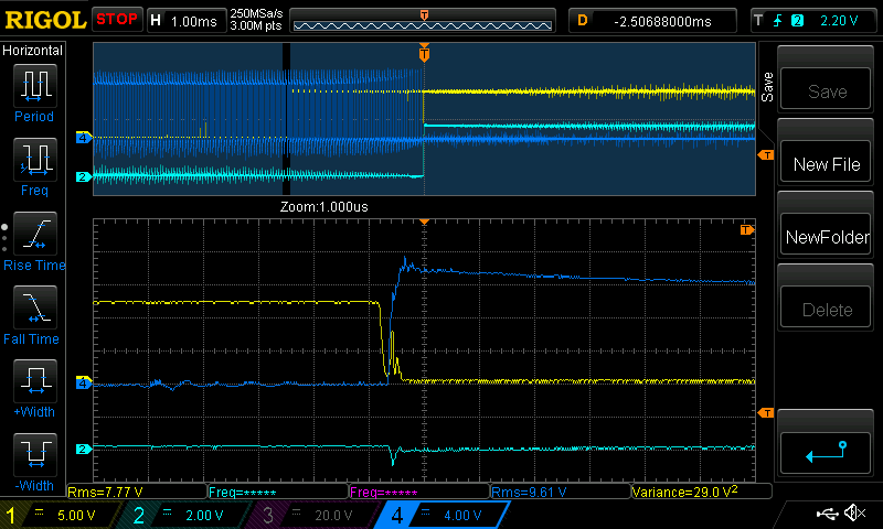
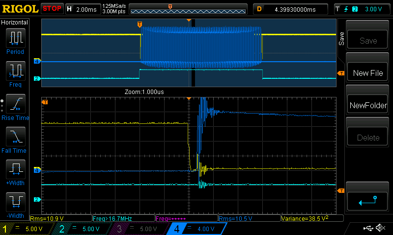
Now we see the new board, with no gate current limiting resistor, nor the diode. I connect the gate direct to the FOD 3182 output pin.
and
certainly we can see much faster switch on and off but there is now a lot of Mhz or more ringing. This is seen in the Dark Blue trace when it goes from low voltage to about 15V, pulling the inverter output up to 54V.
I know that there should be a gate resistor according to just about all power electrics design practice but I wanted to see what it looks like without it.
One aim of this design is to have the smallest amount of "stuff" that makes up the high side gate drive. I wanted to minimise the capacitance and inductance of this by having just the drive side of the FOD3182, it's supply cap and 2 inches of thin PCB trace that follows the high side output as it switches from 0V DC to 54V DC at 20 kHz. I have got what I wanted.
time to see if a 4R7 gate resistor helps things. And after that I will add the 1N4148 for faster switch off.
Posted: 02:05am 09 Feb 2026 Copy link to clipboard
poida Guru
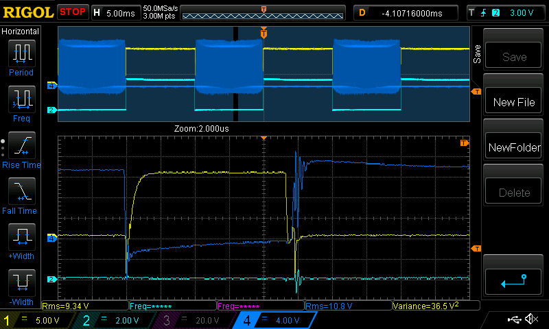
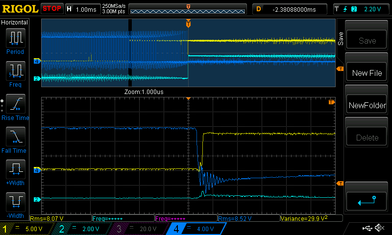
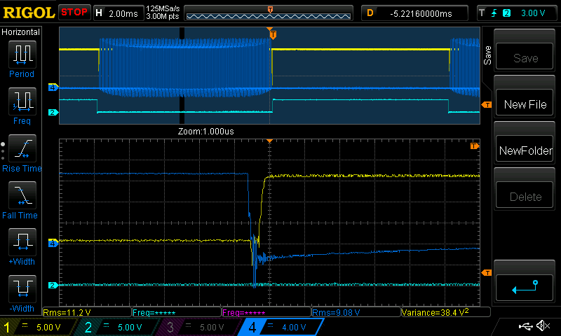
things have changed after fitting the 10R resistor (I had no 4R7)
first, just the resistor:
and
the high frequency ringing is gone. as are the fast gate voltage slopes. This is to be expected, less current into the capacitance of the FET gate will mean slower rise and fall times. And look at the second peaks. this is new to me. I think the diodes will help with those.
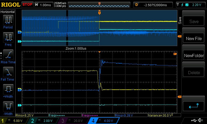
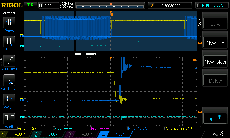
now I also add 1N5819 diodes. These are Schottky type and switch fast, and a voltage drop of about 0.5V
and
now the gate voltages (and therefore the switching performance of the FETs) are looking good. I see very low voltage on the LOW side FET gate after the high side FET switches on, pulling the inverter output up to DC supply voltage. This is when shoot through is most likely.
there still is some high frequency voltage on the high side gate and this is when we start thinking about ferrite beads.
Posted: 02:13am 09 Feb 2026 Copy link to clipboard
poida Guru
here are these waveforms when under 1300W AC output load.
they look not bad and I see they show almost identical features as seen in the above low power testing.
I see the low side gate easily getting high enough to cause some shoot through. maybe it's time to review what I found with ferrite beads since I see some scope for improvement.
Posted: 03:20am 09 Feb 2026 Copy link to clipboard
poida Guru
for reference, here is Wiseguy's gate voltages under the two tests 200 W and 1300 W AC output.
first is 200W:
and
I see the low side gate is being yanked up as the high side switches on. not too much no doubt.
and for 1300 W output I saw this:
and
clearly the low side FET gate is being pulled high enough to make it switch on while the high side FET is switching on. this is shoot through.
overall the voltages seem better controlled than my 1 FET board as seen above.
I probed the gate voltages using the isolated probe and one non-isolated probe which was on the low side FET's gate.
Posted: 05:35am 09 Feb 2026 Copy link to clipboard
Solar Mike Guru
The impedance presented to the gate of the low side mosfet when switched off determines to some degree how high its gate voltage will be pulled up as the high side device turns on.
You could try lowering the gate resistor to 3.5r and see how it performs, and again with the schottky diode in parallel with it.
Another thing to try is placing a small cap 470pf directly across the gate\source of the low side device, this may help with shoot through.
Cheers Mike
Posted: 07:05am 09 Feb 2026 Copy link to clipboard
poida Guru
thanks for the tip I do not have things like 3R5 resistors here at home. it's probably worth a try tho. I wanted to compare the old TIP41/42 thing with the new board so I had to use 10R resistors.
I am curious about the idea of adding capacitance to the Gate. when I add a cap to the gate pin, it still has to "operate" via the pin's lead since this voltage jump is generated from the chip's internal capacitance that is coupled to the drain/source voltage difference. I would guess there is a balance of this and that which could be found that might be just right.
I would love to get right in there and disable this coupling. but it just is there.
Posted: 08:08am 09 Feb 2026 Copy link to clipboard
Solar Mike Guru
That small cap (ceramic) is a very low impedance and can absorb some of the miller pulse getting back into the gate; too large and its going to stress out your driver chip...
AS an experiment: remove the gate drive resistor to one of the L0 mosfets, short the gate directly to its source pin via a similar resistor, this removes the inductance and any transmission line affect back to the driver IC.
Power it up, yeah the output wave form will be crap, but place your scope probe across the shorting resistor, see what gets reflected back by the miller effect as the H0 mosfet turns on; if the wave form is heaps better, then you know its circuit board layout dynamics affecting the gate drive, perhaps necessitating a better layout.
Aim to have the output of the mosfet driver 5-10mm or so from the gate pin, remember the gate circuit is a transmission line, the longer and thinner it is, the more time it takes for the driver transition to get to the gate, similarly a miller pulse getting into the gate from H0 mosfet turning on, takes longer to be negated by the impedance of the driver sitting at 0 volts. Edited 2026-02-09 18:27 by Solar Mike
Posted: 08:12am 12 Feb 2026 Copy link to clipboard
wiseguy Guru
The gate resistors for the HY5608's that I got very good results with are 1R2. I did not get any noticeable improvement by adding diodes across the resistors.
I did use a 12V - 15V low side DC/DC module to provide the negative bias of ~ 3V there was no shoot through at all. The two capacitors across each of the inverse optocoupler LEDs is listed as 1nF, in the 16 FET Power board I used 1n5, maybe 1n is a bit on the small side. The capacitors are proportional to the "dead time" between upper and lower FETs.
If the gate resistor values are too high Miller can try to turn on the FET when it should be off.
The combination of 1R2 low impedance drive and -3V Gate bias has served me well in my builds. Although I did not notice any issues with no negative 3V bias, I do like the belts and braces approach and extra safety margins afforded by using the -3V bias.
If the Wiseguy small FET board was one supplied from me ages ago maybe I put the wrong resistor values in as I had initially decided to just use HY4008's ? They look like 3R3 from the picture?
Posted: 07:14pm 14 Feb 2026 Copy link to clipboard
analog8484 Senior Member
Nice captures of the false turn-on waveforms. The most interesting ones to me are the ones under low load conditions where most inverters spend their time when running. My theory is that frequent (PWM frequency) but short false turn-on's under low/no load conditions are pernicious and cause the thin MOSFET gate oxide layer to degrade over time and can eventually fail suddenly even without a significant load.
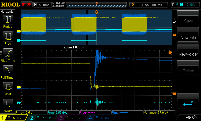
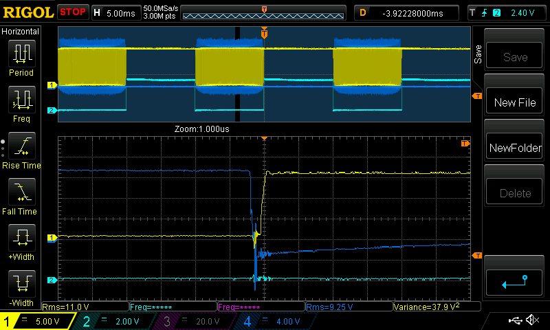
Looking at the 200W load low-side waveforms of the new board:
200W load, no gate resistor or diode:
200W load, 10R gate resistor and diode:
It looks like the false turn-on peaks (~2.5 to ~3V) are greater than the minimum HY4008/HY5608 gate turn-on threshold voltage (2V). Adding a small gate cap should help reduce the false turn-on peak as it changes the overall Cgd/Cgs ratio. However, it also has other side effects like increased switching loss. Perhaps negative gate bias voltage would be the cleaner way to keep the false turn-on peaks well below the minimum MOSFET gate turn-on threshold voltage.
Posted: 01:08am 15 Feb 2026 Copy link to clipboard
poida Guru
I agree with you re. long term low power running with some shoot through is bad for reliability. The failure mechanism is a puzzle for me. I agree failure results when gate oxide layer degrades enough. These FETS are robust in the other areas though so some ST will heat the device and reduce conversion efficiency but leave the oxide layer undamaged?
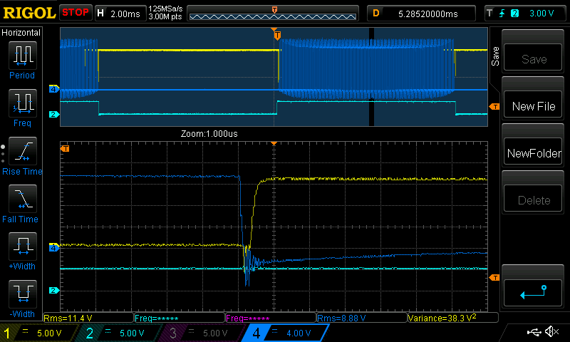
I took above suggestions and tried 1R2 and 2R2 gate resistors (in place of 10R) and on the 2R2 side, I tried 270pF and 470pF caps, connecting Gate to Source with short leads.
more DSO captures again..
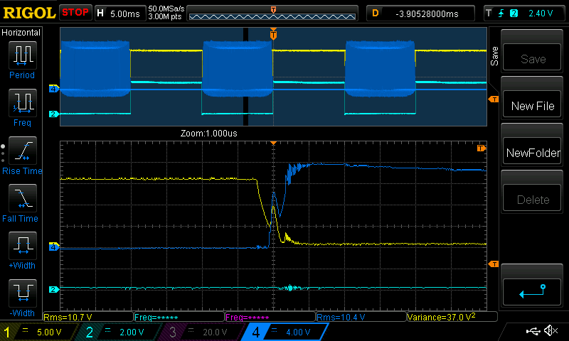
first is 2R2 with no caps
low side switches on (Yellow is low side gate voltage)
high side switches on (dare blue is high side gate voltage) and this is where the trouble is located.
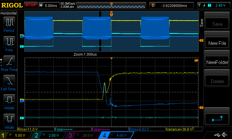
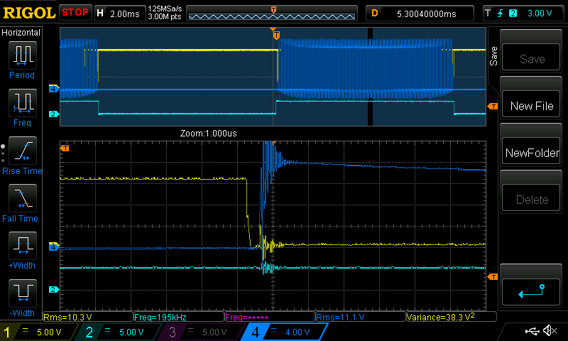
and then there are the 1R2 gate resistors. in both cases switching speeds seem a bit faster.
and
there is a lot of high freq activity on the gate voltages, indicating wild oscillation of the state of the half bridge switching process.
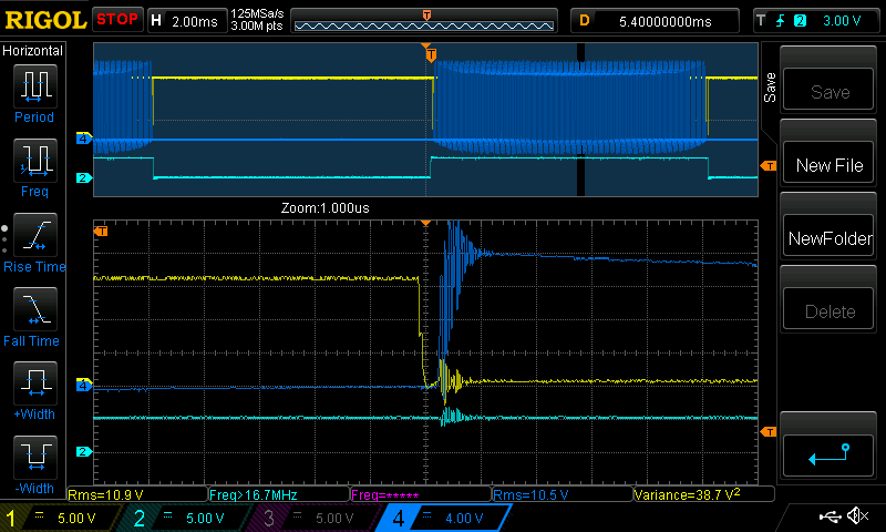
I now put 270pf ceramic cap across the gate and source pins of both low and high side. maybe less oscillations?
and
and now replaced with 470pF caps
and
not a lot of improvement, sadly.
Posted: 01:34am 15 Feb 2026 Copy link to clipboard
poida Guru
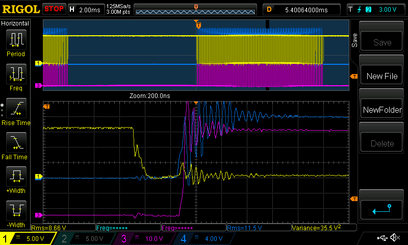
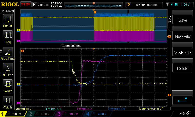
here is a detailed look at high side switch on, this time with 2 470pF parallel across gate and source. this is nearly 1nF.
Pink is half bridge output voltage (connected to primary winding) 125MSamp/sec means 25 sample points each 200ns so the voltages are what the DSO saw (and not implied with interpolation)
The output is ringing like a bell and what is driving it? we know output voltage couples into the low side gate voltage probably there is some inter channel cross talk too.
I like how it rings hard, reduces some, then rings again, then settles down. it seems to be 4 cycles per 200ns or 20Mhz If I could target this with something tuned for 20 Mhz things might start looking good.
the above tests were at 200W output load. this is with no load at nearly the same place in the 50Hz cycle.
I can't believe how good it looks
to see what sort of difference in signal probing I connected the isolated probe to the bridge output and it follows the Pink curve perfectly is a little delayed. similar rise times and delayed by 8ns.
so that voltage on the output rises well before the high side FET switches on. Edited 2026-02-15 11:50 by poida
Posted: 03:24am 15 Feb 2026 Copy link to clipboard
Solar Mike Guru
So adding additional small input caps (gate-source) don't seem to do much; best to remove them.
Going back to your earlier High side scope output, those HF oscillations are there from the start, perhaps place snubber across the H0, H1 mosfets (Drain-Source) to try to reduce their intensity, try 2200pf 500v ceramic cap in series with 6.8R 1 watt resistor. The cap value is usually quite small and depends on the oscillation frequency. Edited 2026-02-15 13:25 by Solar Mike
Posted: 07:16pm 15 Feb 2026 Copy link to clipboard
analog8484 Senior Member
For clarification, were the gate resistor and cap changes made *with* the turn-off bypass diode?
If not, the results showing increased false turn-on peaks are not surprising. From earlier tests, it's clear that the turn-off bypass diode is necessary but *not* sufficient to reduce the false turn-on peak level to below the gate turn-on threshold voltage. This suggests the gate driver internal turn-off resistance is already relatively high. Any external turn-off resistance will only increase the false turn-on voltage. I would suggest adding the 470pF gate cap to the 10R/diode config from earlier tests.
As for failure mechanism, my high level understanding is that shoot-through generates tremendous heat rapidly that degrades the gate oxide layer. Specifically, shoot-through during false turn-on's happens in the linear region of both high and low side FET's which is really bad. This is very different from high load conditions in systems without shoot-through's where the FET's are mostly experiencing high current in the non-linear region. Edited 2026-02-16 05:18 by analog8484
Page 1 of 2
The Back Shed's forum code is written, and hosted, in Australia.