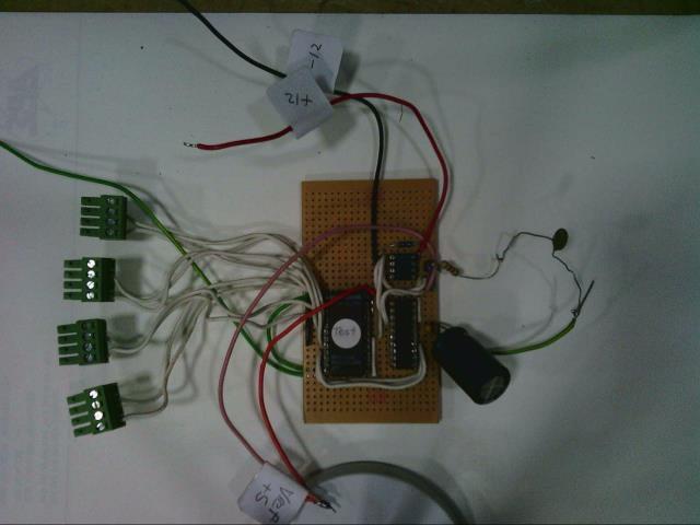
Part 30: MOSFET gate voltages with Madness's power boardNow the nanoverter is running well, I have found it useful for looking at
potential causes of failure with our inverters.
This time I am looking at the dv/dt induced voltage changes at MOSFET gate pins
and the voltages seen at the IR21844 gate drive IC outputs.
I have been very wary of negative voltages appearing on the drive IC outputs.
I suspect these -ve voltages have resulted in inverter failures.
I have no proof, mind, but IR specify Absolute maximum rating for Vlo
as from -0.3V to (Vcc+0.3V).
I have seen Vlo voltages much less than -0.3V in other inverters I tested on the bench.
This has lead me to use and recommend 15V TVS diodes across Vlo to ground and
Vho to Vs (high side gate drive and VS).
Now the Madness power board is built, let's see what voltages appear on the gate drive outputs, now they only need to drive the two transistor base pins, thanks to Madness choosing a on-board totem pole gate drive design.
(yet more DSO screens follow)
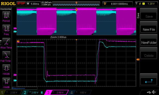
Light Blue is IR21844 gate drive output, sampled very close to the IC pins.
Pink is MOSFET gate voltage
Firstly, no load condition.
Close to the beginning of a 1/2 wave:
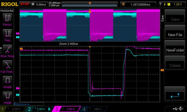
Notice the MOSFET gate exhibits large voltage spikes due to dv/dt (i.e. fast voltage changes at VS)
These spikes do not find their way back to the gate drive IC outputs.
Nice.
Now at the other end of the 1/2 wave:
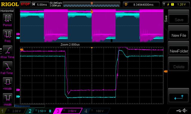
Again, the negative pulse was not seen at the gate drive IC.
Something else to see, there is indication of oscillation when the low side MOSFETS switch ON, to pull VS to ground. This oscillation is also not present on the gate drive IC outputs.
Now, with 150W load, we see near the start:
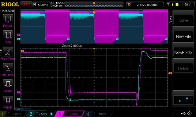
A lot more changes on the gate voltage at the MOSFET.
Look at the huge negative spike just before MOSFET switch ON.
That was completely insulated from the drive IC pin. None of it got through.
We can see more energetic oscillations now, with a bit of load on the bridge.
And near the end of the half wave, under load:
pretty much the same.
I have to conclude that totem-pole MOSFET drive has shown the best, least potentially destructive gate drive voltages on the IR21844 drive chips.
This seems to me to be the way to go in power board design.
Wiseguy has a project using potentially better performing gate drive, made with optocouplers and isolated DC supplies, etc. I look forward to seeing how his design works too.
I think the inverters we have built, using the outputs from the IR2110, direct into MOSFET gates, via a 5R resistor (or something) bring some issues of reliability
thanks to the dv/dt voltage pulses that can damage the gate drive ICs.
My idea of using 15V TVS diodes is a bandaid. It works.
But I think to avoid conveying damaging voltages back to the drive ICs would be the better approach to take by using totem pole drives located close to the MOSFETS.
Totem-pole drive:
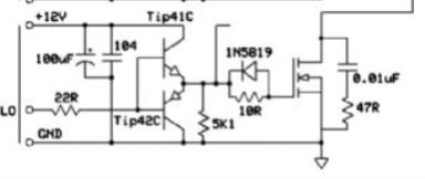
This is a small clip of Tinker's schematic.
The gate drive IC output is fed into the bases of the two transistors via the 22R resistor. If the current is high enough, one transistor will conduct. If the current is low enough, the other transistor will keep conducting. Both won't be conducting for very long. Voltages appearing on their emitters and collectors won't get back to their base pins, as we have seen in the above DSO traces.
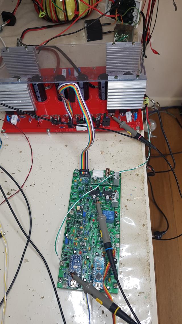
this is how the testing was done:
Looking at the traces again, I see the gate drive IC outputs exceeding 15V, maybe getting to 16.5V. This is not good, I know the IC's have a supply of 15V.
The specs say no more than DC supply + 0.3V
I think we need the TVS or 15V zener diodes after all!
I will put them across the point where the two transistor bases join, and to ground or VS where appropriate.
Edited by poida 2019-03-26
wronger than a phone book full of wrong phone numbers