
|
|
Forum Index : Microcontroller and PC projects : Anyone interested in a new MM+ backpack design?
| Page 1 of 3 |
|||||
| Author | Message | ||||
| Mixtel90 Guru Joined: 05/10/2019 Location: United KingdomPosts: 8788 |
Warning! Newbie Alert! �:) I've got a pcb at an advanced design stage now, but it's a bit different to those I've seen before. It piggybacks behind the ILI9341 with touch screen. The SD card is connected. Chip is PIC32MX470 64-pin TQFP. MCP and DS1307 RTC are on-board. Most IO is on a 16+16 right-angle header off the top so it can be connected by a single ribbon cable if required. The signals aren't necessarily in the order that you'd expect them but that shouldn't matter in this case. The connector includes all the SSD1963 signals so a bigger display can be used. COM1, COM2 & COM3 are included, as are PWM1A, PWM1B and PWM2A. The connector includes +5V and GND so the device can be powered through the ribbon. Alongside the IO connector are a 4-pin console connector and a PS2 keyboard socket. On the LH side are a reset button and mini USB connector. Along the bottom are two LEDs and an Auxiliary IO header. The first LED is for 3V3 indication, the second has dual function as SD card enabled and can also be switched by the dedicated RB2 pin. Auxiliary IO includes PB10, RB4, SQW, +3V3, GND, SDA and SCL. A link could be fitted between RB4 and SQW to get the square wave output from the RTC without any additional wiring. A 2-position link selects +5V from either the IO connector or the USB connector. The console +5V is always connected, so leaving the link off would leave power from the console only. This has been fun as I've hand-routed the board even though I've used the free version of Eagle. :) Most of it is SMD. It is, of course, a completely untested design and I haven't sorted out the silk screen or even run a DRC on it yet. :) If anyone is still interested after ploughing through that lot, I'll find a way of sorting out a picture or two. --Mick Edited 2019-10-09 18:42 by Mixtel90 Mick Zilog Inside! nascom.info for Nascom & Gemini Preliminary MMBasic docs & my PCB designs |
||||
bigmik Guru Joined: 20/06/2011 Location: AustraliaPosts: 2980 |
Hi Mick (Another bloke with a great name), Welcome to the Back Shed. Great job on designing your own board.. I was going to do a 470 based board but I decided to opt instead for a MM-Extreme based 64 pin chip. There are two varieties a small 50mm x 50mm PCB and a larger backpack for an SSD1963 display. I am still working on them and have them at a near final stage but have to add a reset switch and clean up the overlays before I send them off.. Here is the stage I am at now.. 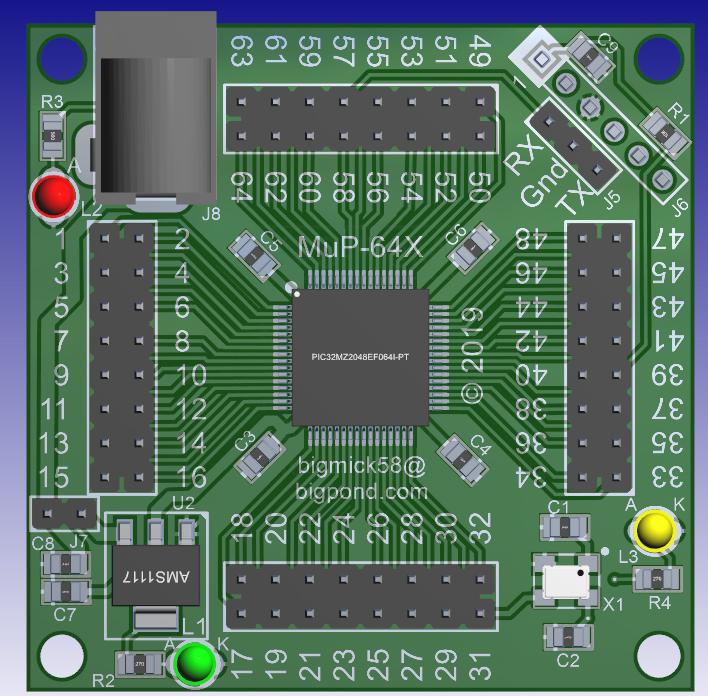 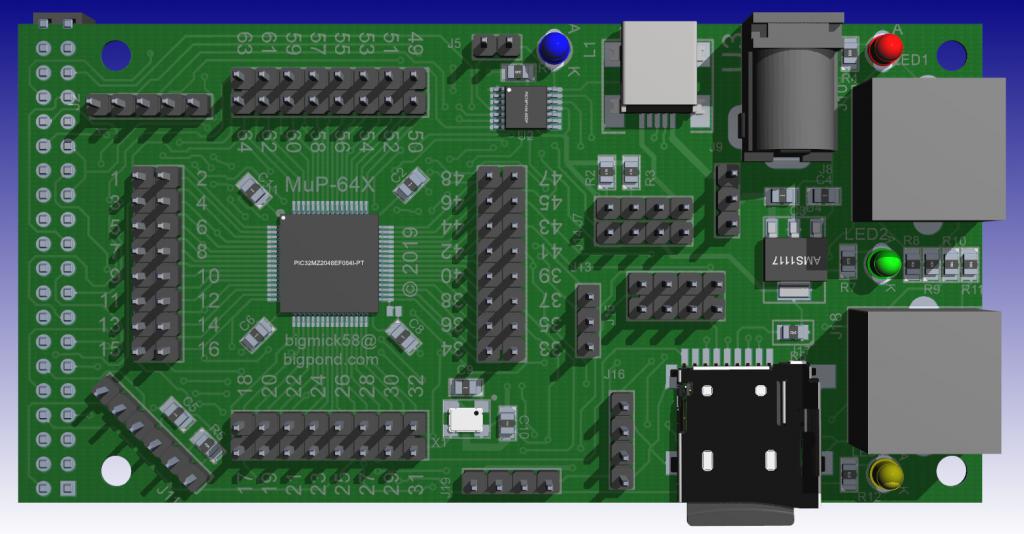 There are several compromises I have made and RTC was one. I really just wanted a faster version of my MuP-Ver3 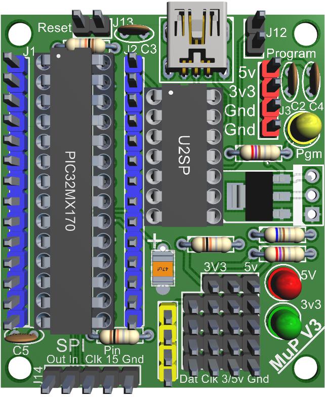 Anyway I am look forward to seeing what you have come up with. Kind Regards, Mick (One of the `others') Mick's uMite Stuff can be found >>> HERE (Kindly hosted by Dontronics) <<< |
||||
| Mixtel90 Guru Joined: 05/10/2019 Location: United KingdomPosts: 8788 |
I hope you'll bear with me. :) This is the first time I've really used Eagle, although I did once have a short play with KiCAD. It's the first time I've laid out a double sided board and the first time I've laid out a SMD board. :) I tried the autorouter but it seemed to be a lot of hassle so I just routed the thing myself. As I said, this is still work in progress. One of those where I think "I wonder if I could add that, make this better or lay that bit out more efficiently!" I've left the copper pours off the pic for clarity, although they do work (and it's the first time I've used those too...).  And I've just discovered that you can't use a "+" sign in a filename. It's taken me ages to find that... �:( And a circuit... 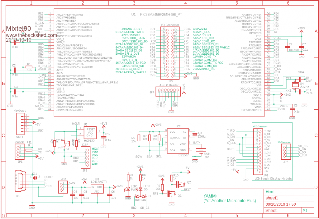 Edited 2019-10-10 02:54 by Mixtel90 Mick Zilog Inside! nascom.info for Nascom & Gemini Preliminary MMBasic docs & my PCB designs |
||||
| bigmik Guru Joined: 20/06/2011 Location: AustraliaPosts: 2980 |
Hi Mick, I used DEXPCB (Formerly AutoTrax-DEX). The free ELECTRA autorouter (no longer available, I believe but mine still works) has a limit of 250 pads. Mine exceeded that very quickly so I laid mine out by hand.. It is always an issue of what to add or what to omit.. There is no one size fits all solution as you need a larger board to accommodate every taste and I am sure that even then there will be compromises that some will not like. I had some discussion about adding a Winbond RAM chip but I omitted it (mainly due to insufficient IO pins that aren't used for other functions. I have catered for those you need the ram function to use the TFT screen optional RAM chip. Hmmm I suppose I could reuse that IO pin as only one or the other can be used at the same time... I will look into that option. Looking forward to hearing how your PCB comes out (I have a couple of 470's sitting here) Kind Regards, Mick Mick's uMite Stuff can be found >>> HERE (Kindly hosted by Dontronics) <<< |
||||
Grogster Admin Group Joined: 31/12/2012 Location: New ZealandPosts: 9939 |
YAMM+ Catchy name!  Nice looking board. You did well for a first time double-sided SMD board. When you have built one, please post more photos. Smoke makes things work. When the smoke gets out, it stops! |
||||
| led-bloon Senior Member Joined: 21/12/2014 Location: AustraliaPosts: 209 |
Mick or Grogster should know.. Would a PIC16F1455 for programming and serial console be good addition? led Miss you George |
||||
| WhiteWizzard Guru Joined: 05/04/2013 Location: United KingdomPosts: 2967 |
Hi Mick, I would definitely recommend a Microbridge onboard - it then future-proofs the design (in terms of easy Firmware upgrades). I would also recommend replacing the DS1307 with a way-more accurate DS3231. Based on the 64pin MM+, this would make a very nice replacement for the SC featured module which costs a fortune for the PCB from SC. Hope this helps! WW |
||||
| bigmik Guru Joined: 20/06/2011 Location: AustraliaPosts: 2980 |
G�day Phil, grogster, I agree, I would not, generally, design a new �mite without a micro bridge onboard.. If you look at the larger of my boards you will see the pic16 micro bridge just under the blue LED (top middle) SSOP package. The smaller pcb doesn�t have it yet but I have put that one aside to finish the larger one.. It may end up being needing a plug-in daughter board that has all the other goodies on board, this would make a very small package 50mm x 50mm x about 25mm high Since posting I think I have finished the larger (50x100mm) board, which I call BackPack-64X (64 Extreme). I have added a reset switch and a WinBond memory chip since the picture above. I will have a look at adding a RTC. It is amazing how hard it was to assign IO for the devices as there are only a few that aren�t used for com or sound or other devices.. I have used all the available COUNT pins and all of PWM port 1 Pins.. I wondered about adding the ICSP header but it was easy enough to squeeze it in.. in fact I am not sure if I can use it with the micro bridge fitted. I have to go to hospital for some serious work on my shoulder (15Oct) so I will be in a sling for 4-6 weeks.. I am hoping to get them off to the pcb fab house before then. Regards, Mick Mick's uMite Stuff can be found >>> HERE (Kindly hosted by Dontronics) <<< |
||||
| Mixtel90 Guru Joined: 05/10/2019 Location: United KingdomPosts: 8788 |
The mods are going well. :) I've dumped the ICSP header. I doubt if it'll go back now. I've used the DIL microbridge so it could easily be unplugged to get access to the ICSP signals if necessary, possibly using a 14DIP header. I'm not sure about leaving the MCP on now. Does the microbridge replace that? It could give MCLR a low pulse on startup as it has the signal available. Those are rather lovely boards, Mick! :) --Mick Edited 2019-10-12 02:04 by Mixtel90 Mick Zilog Inside! nascom.info for Nascom & Gemini Preliminary MMBasic docs & my PCB designs |
||||
| bigmik Guru Joined: 20/06/2011 Location: AustraliaPosts: 2980 |
Hi Mick, (geez this seems like I am talking to myself), I would not omit the mcp120, whilst not critical IMHO, if using a good power supply it would be very beneficial if the power supply was a bit dirty.. I would leave it.. that said I don�t use it on any of my boards... The main thing that made me shy away was the 4 different possible pinouts on the TO92 device.. Regards, Mick Mick's uMite Stuff can be found >>> HERE (Kindly hosted by Dontronics) <<< |
||||
| Mixtel90 Guru Joined: 05/10/2019 Location: United KingdomPosts: 8788 |
Hmmm... Perhaps I should have called this one "Topsy". It just growed... Now there's an optional, socketed, PIC16F1455 microbridge. The ICSP connector is still there, but non-standard 2x3 as I consider it unimportant (and it was the easiest way to keep it!). It's also useful for extending the SD card to an external one, as it carries +3.3V, GND and 2 signals that could be used for WP and CD, the remaining signals are on the existing connector. There's a DS3231 RTC with battery backup. The SQW/INT output is available on a pin. As there's no RAM on the DS3231 I've added a 47L16 SRAM with EEPROM backup, set for auto store. The on-chip USB isn't used now (I don't think there's a way of routing it to anywhere useful now), so one of the pins is used for the HS signal to force a manual store. I didn't point it out before, but the 1k protection resistor is on the console RX pin. 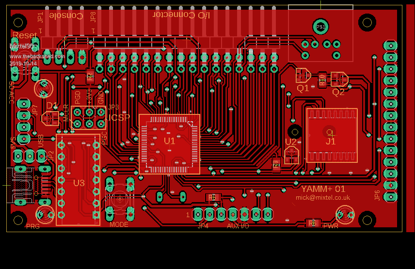 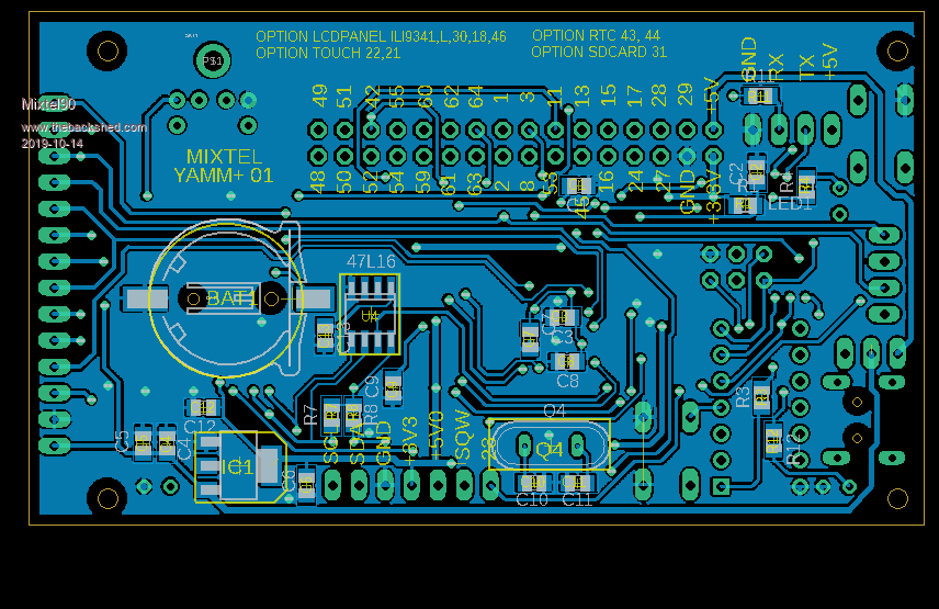 Mick Zilog Inside! nascom.info for Nascom & Gemini Preliminary MMBasic docs & my PCB designs |
||||
| Volhout Guru Joined: 05/03/2018 Location: NetherlandsPosts: 5863 |
Nice layout, I would remove the "floating" ground sections on the red layer (right of U1, and at R9). Smart thinking by patching groundplanes together through the switch. If you could move via's a little bit you could have the ground plane conduct from left to right (blue layer) at C3/C8. Does IC1 get warm ? The MX470 could draw over 100mA. If you put a via close to U3 pin 8, you stitch top and bottom ground planes together. Regards, Volhout PicomiteVGA PETSCII ROBOTS |
||||
| Mixtel90 Guru Joined: 05/10/2019 Location: United KingdomPosts: 8788 |
Thanks, Volhout, that was very helpful. I've done those mods - after finally figuring out how to stitch using vias. I'd left the top layer fill orphans on too. I also discovered that I was putting my silk screen on the wrong layers - I hadn't realised how it worked. I told you I was a beginner at this pcb lark. :) The regulator is a version of the 1117. Apparently the SOT-223 package is ok for about 700mW without any heatsink. Say about half that for safety. With a voltage drop of 1.7v that should allow for 200mA. I've put thermal vias underneath it and moved tracks to get a bit more copper area around there now, so I think I'll be safe even if a bit more stuff gets powered from this board. I looked at it and thought there was something not quite right... Yep, I'd made the board 0.05" too narrow so the LCD connectors and fixing holes weren't on the centre line! Fixed that too, and double checked the LCD connector positions and fixing holes. It's given me a smidgen more board space. :) Does anyone think it would be an idea to sacrifice the user-controlled LED (to use as the EERAM HS signal)and wire the 470's on-chip USB out somehow? Even if it's only to a header. Mick Zilog Inside! nascom.info for Nascom & Gemini Preliminary MMBasic docs & my PCB designs |
||||
| Volhout Guru Joined: 05/03/2018 Location: NetherlandsPosts: 5863 |
Hi Mixtel90, I would leave the user controlled LED on. If the autostore in the 47L16 works OK there is absolutely no reason to force additional stores. That being said, you do need a large enough capacitor for these stores to succeed (for the 47L16 that is 10uF (typical). Make sure you have effectively 10uF at the Vcap pin. In the layout it looks like there is an 0805 package ceramic cap at 47L16 pin 1. Ceramic capacitors have voltage derating. See derating curve for a 0805 10uF ceramic cap. A 10uF part is effectively 8 - 9uF at 3.3V. At higher voltages derating is even more. 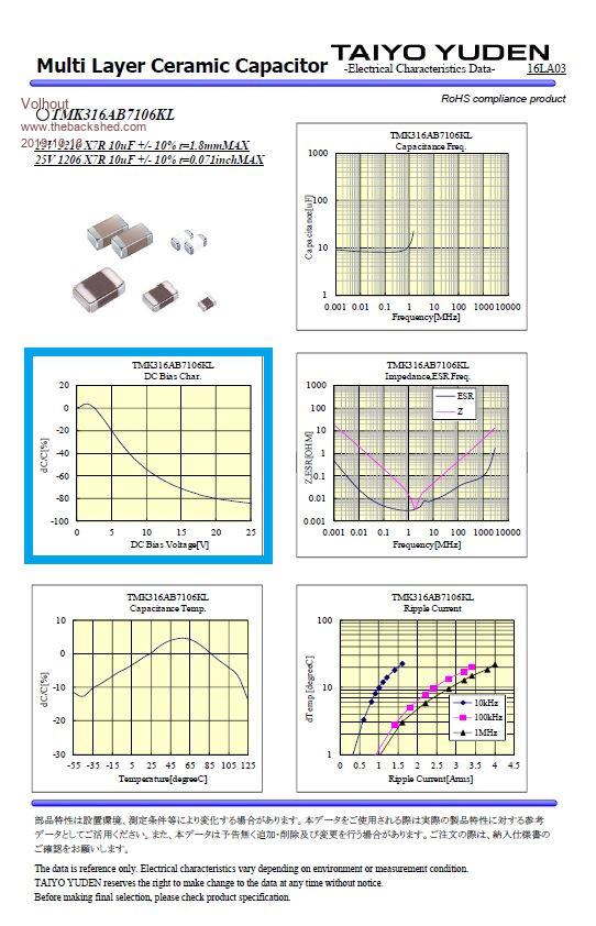 The MX470 USB pins.. It will be hard to get 5V to a header at these pins (try routing it). You could offer two solder pads at D+ and D-, that if desired people can wire to a USB connector. Regards, Volhout P.S. sign me up for 1 board if you order... Edited 2019-10-16 17:52 by Volhout PicomiteVGA PETSCII ROBOTS |
||||
| Mixtel90 Guru Joined: 05/10/2019 Location: United KingdomPosts: 8788 |
Oh, very useful information! The capacitance drops pretty quickly, doesn't it? Fixed it now. The ceramic might have just about worked (8uF min), but it would have been borderline with a 47L16. As a max value isn't given, I've swapped it for a 22uF tant - or anything else that will fit those slightly bigger pads. The HS signal has gone now, but I might run it to a pad just in case someone wants to get to it. I managed to route the chip USB to the Aux I/O header, although I think I should find somewhere to put a link to the 5V rail. There might *just* be space. One of the advantages of being retired is that I can have serious time to play. :) In the schematic the 47L16 is using the wrong pic. I couldn't find an Eagle library with one in and I can't be bothered creating one at the moment. The pin numbers and footprint are right, but that's a 24 series, I think. :) Just in case you were wondering about the cap on A0... 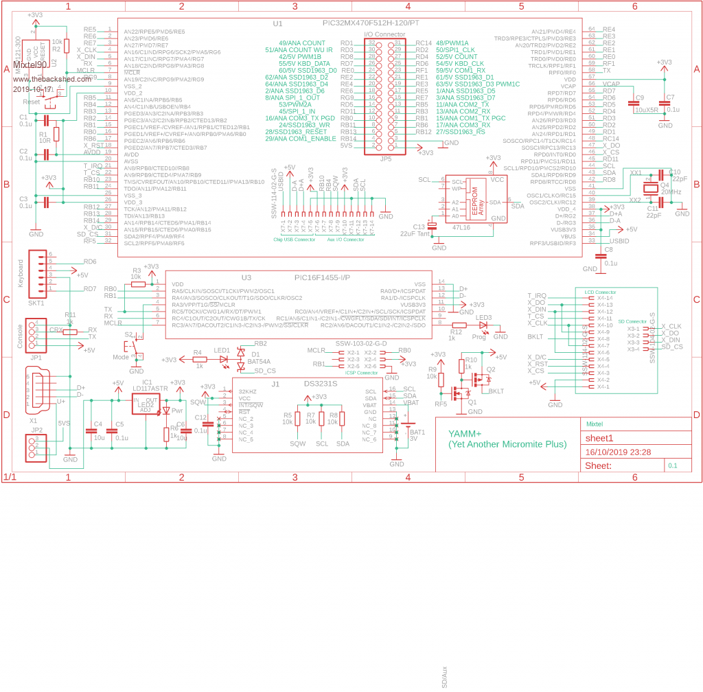 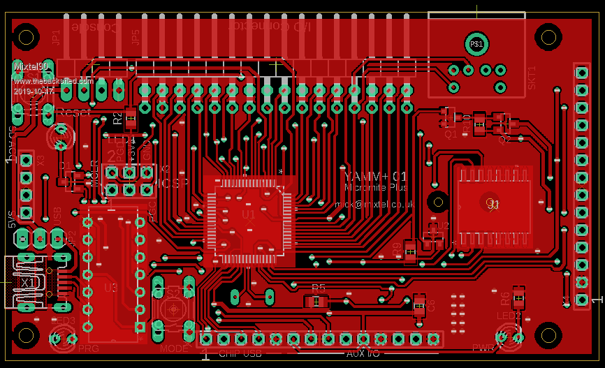 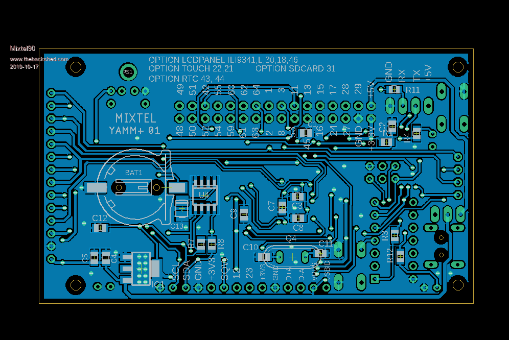 You're on the list. :) Mick Zilog Inside! nascom.info for Nascom & Gemini Preliminary MMBasic docs & my PCB designs |
||||
mikeb Senior Member Joined: 10/04/2016 Location: AustraliaPosts: 178 |
Great job. Just a suggestion. Bring AVdd and AVss pins out via a linked header. This way you allow the user to isolate from the onboard RC network and connect to a stable/clean analogue supply. Just my 2 cents worth. Once again. Great job. Regards, Mike B. There are 10 kinds of people in the world. Those that understand binary and those that don't. |
||||
| Mixtel90 Guru Joined: 05/10/2019 Location: United KingdomPosts: 8788 |
hehe, Mike. I know what you did. You looked at the most awkward area of the board and suggested something clunky to go in there. ;) I can half do it. A 3-pin 2.54mm header with the RC supply, AVdd and GND/AVss on the pins. I've not found enough space to isolate AVss, but being able to connect the external 0V to ground at the 470's pin should be enough, I think. I've drawn it as a female header, but that was just to get smaller pads. It would probably be a male header with a link. I might be able to isolate AVss if I use a 2mm or 1.27mm header & link, but it would be harder to connect an external supply to. Don't you learn to love "ripup @;"? It's rapidly becoming one of my favourites. :) Mick Zilog Inside! nascom.info for Nascom & Gemini Preliminary MMBasic docs & my PCB designs |
||||
| Mixtel90 Guru Joined: 05/10/2019 Location: United KingdomPosts: 8788 |
Right. HS is now on a pad in case anyone wants it. Manual/Auto mode for the EERAM is user selectable by solder link. The SD / User LED is now a bi-colour 3-pin. Have changed the buttons for the 2-pad SMD sort to save some space. Quite a bit of general tidying up of some of the trackwork. I think I'm close to ordering some boards now. ERC & DRC both pass. -- Mick Mick Zilog Inside! nascom.info for Nascom & Gemini Preliminary MMBasic docs & my PCB designs |
||||
| Mixtel90 Guru Joined: 05/10/2019 Location: United KingdomPosts: 8788 |
The PIC16F1455 and prog LED are now smd and the ICSP connector has gone. That left a little space for me to play with. :) Some may wonder why the other LEDs are through-hole. The idea is that they could be more easily mounted externally if required. From the beginning I've intended that this board could be built in different ways depending on how the user wants to use it. The 90 degree IO connector could be vertical pins off the front or the back, for example. Have added a micro SD card socket (on bottom side, just to the left of USB2) so that one is available with an external display. It has its own select line. Also changed the wired-out chip USB to a second mini USB socket. Quite a bit of IO pin rewiring has grouped the SSD1963 pins, COM 1-3 ports, the 3 PWM pins, 3 count pins and SPI1 more or less together. Just because I could. :) 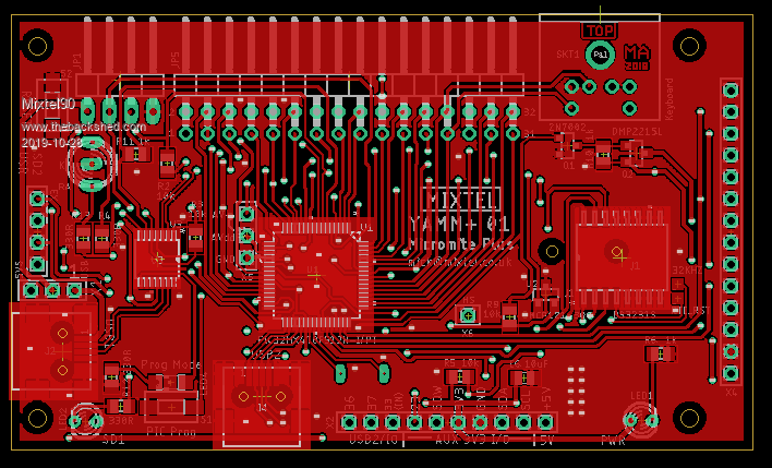 Mick Zilog Inside! nascom.info for Nascom & Gemini Preliminary MMBasic docs & my PCB designs |
||||
| Page 1 of 3 |
|||||
| The Back Shed's forum code is written, and hosted, in Australia. | © JAQ Software 2026 |
