
|
|
Forum Index : Microcontroller and PC projects : PicoMite VGA Edition PCB - release version
| Page 1 of 6 |
|||||
| Author | Message | ||||
| matherp Guru Joined: 11/12/2012 Location: United KingdomPosts: 11673 |
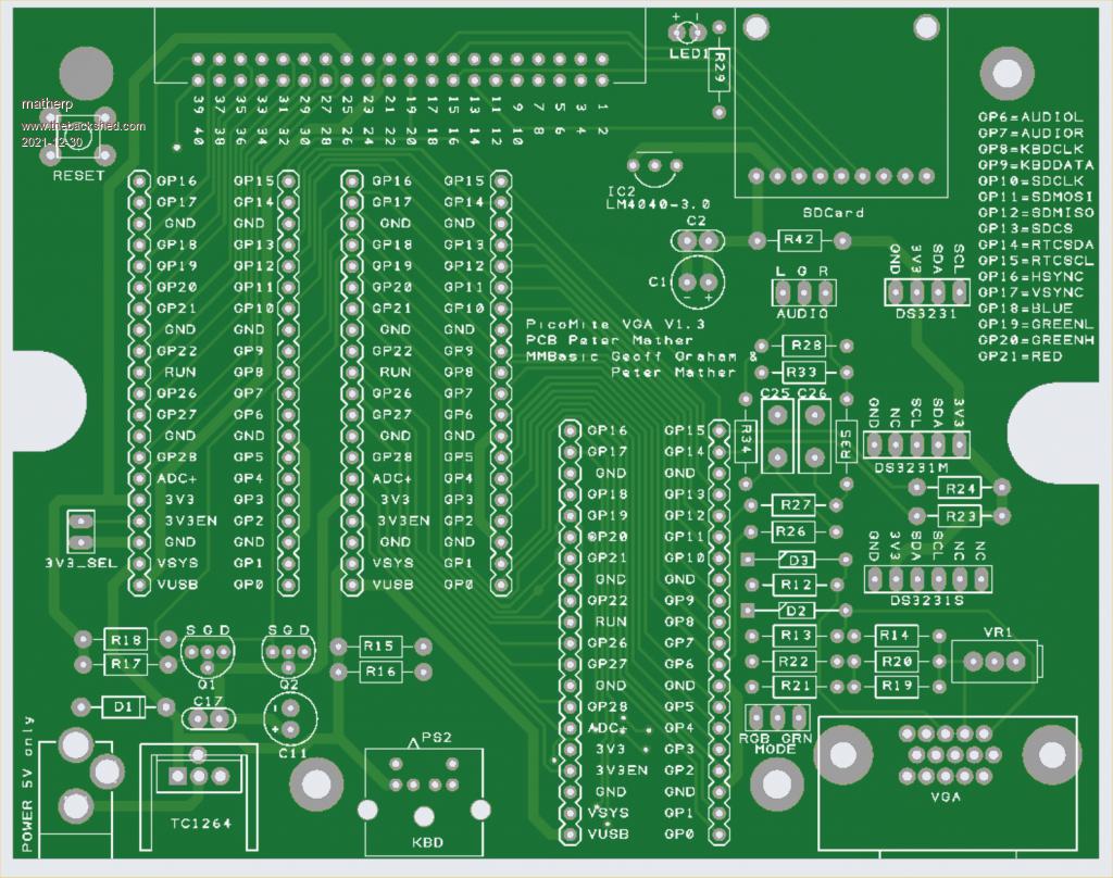 PicoMiteVGA.zip Attached in the ZIP are the DesignSpark design files, the BOM, a printable schematic and a zip containing the gerbers. NOTES: Use a jumper on the 3V3_SEL header to disable the PicoMite power supply if you want to use the onboard linear supply. With the header in place you can power the board through the 2.1mm power connector or with the USB connection to the Pico. Both supplies have an in-line diode so it doesn't even matter if both are connected. The MODE header selects between RGB/mid intensity green mono if in the left position and full intensity green mono in the right position. the header could be connected to a panel mount changeover switch if required The mosfet footprints are for a BST72A which is the device tested. If using another n-channel enhancement mosfet be sure to match the source, gate and drive to the silkscreening. Any mosfet must meet the requirements specified in AN97055 The audio header can be connected to a panel mount 3.5mm audio socket The SDcard module can be mounted on a header or direct soldered to the board as in the picture Solder header pins into the 2 extra Pico pinouts to mount Pico shields direct on the PCB The RTC headers support both the major types of DS3231 modules available. I prefer this version as it has a larger and widely available replaceable battery All option configuration is specified on the silkscreening on the bottom of the PCB Many components are optional - see the BOM for details If the LM4040-3.0 is fitted ensure that you include OPTION VCC 3.0 in any programs using the ADC Adjust VR1 to get the best white balance when in colour mode I'll post dxf files for end panels for the case at a later date FINALLY enjoy the complete b....ks I made of the PS2 connector in my prototype  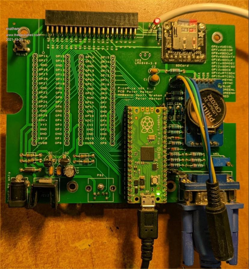 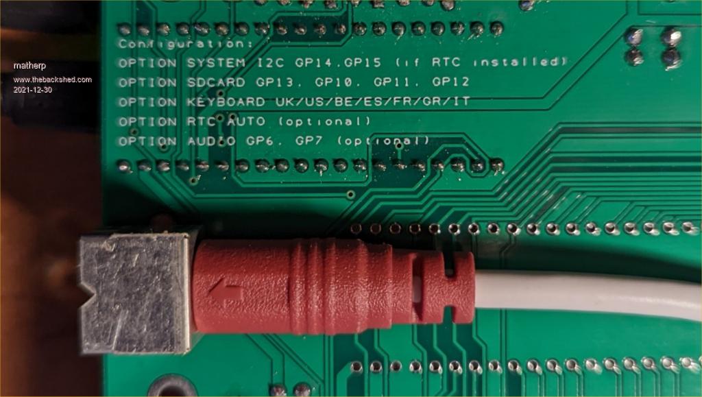 Edited 2021-12-30 05:51 by matherp |
||||
| Mixtel90 Guru Joined: 05/10/2019 Location: United KingdomPosts: 8981 |
Thank you, Peter. Now I know that I'm not alone when I totally screw something up and it makes me feel better about it. :) Don't feel too bad about this. One of my current projects is a Nascom-4 (it simulates an expanded Nascom-2 using a FPGA). The designer of the board also crossed over the PS/2 connections so now it's mounted on the bottom. :) I currently have 5 of the mini PCBs on the slow boat from China - all with messed up connections to the PS/2 skt. It's a track hack to fix that though. Nice board. :) You'll be pleased to hear that I've at least got as far as downloading DesignSpark 10. lol Mick Zilog Inside! nascom.info for Nascom & Gemini Preliminary MMBasic docs & my PCB designs |
||||
mobluse Newbie Joined: 10/02/2013 Location: SwedenPosts: 24 |
Can you also connect a PS/2 mouse to this using a PS/2 Y-splitter cable? And use the PS/2 keyboard at the same time? Maker Pi Pico Rev1.2, DuinoMite-Mini, Raspberry Pi 0-4, iCE40HX8K, Arduino Uno, VM111, STK500, ZX81 |
||||
| matherp Guru Joined: 11/12/2012 Location: United KingdomPosts: 11673 |
No, mouse is not supported and would need different pins anyway |
||||
| phil99 Guru Joined: 11/02/2018 Location: AustraliaPosts: 3325 |
Laptops that use the PS/2 Y-splitter cable have the mouse socket clock and data lines wired to the two spare pins in the plug, with the laptop having two PS/2 controllers, same as a desktop. |
||||
| robert.rozee Guru Joined: 31/12/2012 Location: New ZealandPosts: 2542 |
hi peter, a couple of quick questions: 1. the 40-way connector (J3 on your schematic), does each row of pins on the physical connector correspond to one side of the pico? this is how it is depicted on the schematic, but NOT how the pins are numbered on the PCB. 2. can the RTC I2C bus be shared with other I2C devices that the user attaches? cheers, rob :-) |
||||
| matherp Guru Joined: 11/12/2012 Location: United KingdomPosts: 11673 |
No the numbering on the silkscreen should be correct and relates to the Pico as a standard DIL chip with GP0 as pin1 and VBUS as pin 40 Yes. You can't use open and close but read and write will both work Edited 2021-12-31 00:07 by matherp |
||||
| robert.rozee Guru Joined: 31/12/2012 Location: New ZealandPosts: 2542 |
so the layout (looking into the connector from the front) is something like the below? (1) (2) GP0 x x GP1 GND x x GP2 GP3 x x GP4 GP5 x x GND GP6 x x GP7 GP8 x x GP9 GND x x GP10 GP11 x x GP12 GP13 x x GND GP14 x x GP15 GP16 x x GP17 GND x x GP18 GP19 x x GP20 GP21 x x GND GP22 x x nRST GP26 x x GP27 GND x x GP28 ADCREF x x 3v3 3v3EN x x GND VSYS x x VUSB (39) (40) cheers, rob :-) Edited 2021-12-31 00:44 by robert.rozee |
||||
| matherp Guru Joined: 11/12/2012 Location: United KingdomPosts: 11673 |
Exactly so. We can include that as a picture in the manual when written |
||||
| JohnS Guru Joined: 18/11/2011 Location: United KingdomPosts: 4357 |
I'm struggling to understand the above - isn't it wrong? Am I mixing up the CPU pinout and whatever J3 is? Also, looking at the schematic, VGA looks to be shown as 17 pins but isn't it a DB15? (or some such name) John Edited 2022-03-22 03:38 by JohnS |
||||
| matherp Guru Joined: 11/12/2012 Location: United KingdomPosts: 11673 |
John The pin numbers on the connector are exactly the same as the Pico BUT the layout of the connector is completely different. See the pic of the board at the top of the thread which shows the pin numbers on the connector. I could have used the Pico layout but then everyone would have complained the the pin numbering on the connector was non-standard (can't win on this one  ) ) |
||||
| JohnS Guru Joined: 18/11/2011 Location: United KingdomPosts: 4357 |
Oh - thanks. What about the other point? The 17 pins / DB15 (DE15)? BTW thanks also about the Gerbers, which JLCPCB did indeed accept without issue. John |
||||
| matherp Guru Joined: 11/12/2012 Location: United KingdomPosts: 11673 |
The two locating pins are counted so 15 normal and 2 locating |
||||
| JohnS Guru Joined: 18/11/2011 Location: United KingdomPosts: 4357 |
Oh. Thanks. John |
||||
| Volhout Guru Joined: 05/03/2018 Location: NetherlandsPosts: 5999 |
@Peter, Is there any objection to wire the green VGA pin similar to red and blue (in essence use GP20, and do not connect GP19?) for an 8 color wiring ? Or should I use GP19 and not use GP20 ? And will this wiring be compatible with 640x480 ? Another question: is the SD card bit-banged (in other words, can I swap pins around?) or are they using the SPI hardware inside the pico ? In that case MISO, MOSI, CLK pins are fixed. Thanks for your response Volhout Edited 2022-04-19 19:33 by Volhout PicomiteVGA PETSCII ROBOTS |
||||
| matherp Guru Joined: 11/12/2012 Location: United KingdomPosts: 11673 |
You can but it won't mean you can use the extra pin. If you are trying to simplify the wiring just use a single resistor on gp19 and another on gp20. Play with values to get the white balance and colour gradation. Page 8 |
||||
| Volhout Guru Joined: 05/03/2018 Location: NetherlandsPosts: 5999 |
Yes, this was a clear RTM.... both questions. Thanks for responding anyway... Volhout PicomiteVGA PETSCII ROBOTS |
||||
| Volhout Guru Joined: 05/03/2018 Location: NetherlandsPosts: 5999 |
Yes, this was a clear RTM.... both questions. Thanks for responding anyway... Volhout PicomiteVGA PETSCII ROBOTS |
||||
| phil99 Guru Joined: 11/02/2018 Location: AustraliaPosts: 3325 |
@Volhout "If you are trying to simplify the wiring just use a single resistor on gp19 and another on gp20. Play with values to get the white balance and colour gradation." 330R for green high and 680R for green low works well, along with 220R for red and blue. For my monitor this gives a small overdrive which it clips to 100% so the white balance is good. Edit. Works equally well for both VGA modes. . Edited 2022-04-19 22:54 by phil99 |
||||
| Volhout Guru Joined: 05/03/2018 Location: NetherlandsPosts: 5999 |
Just build the board, and I like the green 640x480 mode a lot. Only 8 colours in colour mode but that is perfect. Now I have my platform for the contest. Thanks turbo46, peter and geoff. PicomiteVGA PETSCII ROBOTS |
||||
| Page 1 of 6 |
|||||
| The Back Shed's forum code is written, and hosted, in Australia. | © JAQ Software 2026 |
