
|
|
Forum Index : Microcontroller and PC projects : Sprint Layout
| Author | Message | ||||
| Mixtel90 Guru Joined: 05/10/2019 Location: United KingdomPosts: 7870 |
Hehe.... :) I found it useful when I had a catastrophic USB stick failure (a new stick - lots of files were still there but corrupted) and discovered that my backup didn't have that particular file on it. I did have the Gerber set though, so I was able to "rescue" the board. Yep, it's not a perfect solution and it takes a little time, but I think it was better than redesigning from scratch or working from a JPG (which doesn't show the bottom tracks very well). The answer is obviously to make sure that your backups are up to date NOW, not in an hour's time or tomorrow. Not always easy to arrange. Mick Zilog Inside! nascom.info for Nascom & Gemini Preliminary MMBasic docs & my PCB designs |
||||
Grogster Admin Group Joined: 31/12/2012 Location: New ZealandPosts: 9593 |
Yeah, I've been bitten by that also in the past, so now I always do three backups of any file I am working on - not just CAD, but word docs or spreadsheets etc. One saved locally to the PC, one to a backup USB flash-drive, and one to the cloud - Dropbox, in my case. I also have an iDrive account, which auto-syncs all files every few days, and I also have a backup server in the shed also. Overkill? Perhaps. But it just saves so much pain if your PC dies or your only flash-drive copy dies etc, and you lose your work and have to do a "Page-one rewrite" kind of thing - never a nice experience, I can tell you. "Multiple redundant backups" should be something EVERYONE does with any file you spend any kind of serious time on. Smoke makes things work. When the smoke gets out, it stops! |
||||
| Tinine Guru Joined: 30/03/2016 Location: United KingdomPosts: 1646 |
 for Dropbox. My system is sync'd, also to my Google Drive. for Dropbox. My system is sync'd, also to my Google Drive.The cool thing about Dropbox (paid-for) is that it keeps an archive of older versions of the file. I have a brain-fart and delete...No problem because Dropbox still has it plus something like 7 (?) prior versions of that same file. Craig |
||||
| matherp Guru Joined: 11/12/2012 Location: United KingdomPosts: 10245 |
And you have the option of rewinding a directory to an earlier time. Allows me to do speculative changes across multiple files and back them out if any issue. My set up is a PC with all drives mirrored, all development areas linked to dropbox, and then a Synology NAS doing incremental disk backups and system drive snapshots. Edited 2022-06-30 19:57 by matherp |
||||
| pwillard Guru Joined: 07/06/2022 Location: United StatesPosts: 313 |
I realize this is a bit off-topic... But I ended up using a spare raspberry pi to create a LOCAL private github-like server using Gitea. So now I have a local copy of the projects I'm working on AND the ability to move to a different PC and still work on them. It removed the need to rely on cloud services like Dropbox or Google drive. (without the sharing with other people features, of course) |
||||
| pwillard Guru Joined: 07/06/2022 Location: United StatesPosts: 313 |
More parts... trying to not overlap what's been shared already... 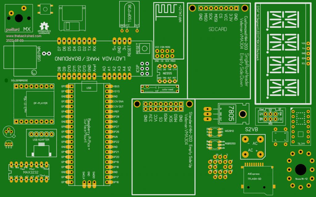 PARTS.zip |
||||
| pwillard Guru Joined: 07/06/2022 Location: United StatesPosts: 313 |
And 1 more... 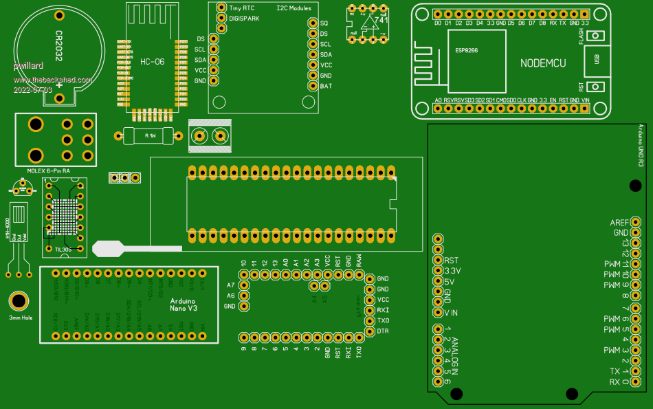 PARTS.zip |
||||
| Volhout Guru Joined: 05/03/2018 Location: NetherlandsPosts: 5058 |
Nice !! PicomiteVGA PETSCII ROBOTS |
||||
| Sasquatch Guru Joined: 08/05/2020 Location: United StatesPosts: 377 |
Well, let me tell you how we did it in the good-olde-days. Some of you may recall or have similar experience. But this is mostly a short history for the younger engineers. If you aren't interested, just scroll on by! No need for sarcastic remarks! So in the old days we used to lay out PCB's on velum paper or textured mylar with 1/10 inch grid. The layout was done at 2X (2:1) actual size and later reduced by a giant graphic arts camera. First we would rough draw the pads with a template and draw the traces in pencil using a different color (colour) pencil for the traces on each layer. It was common practice to run the traces mostly horizontally on the top (component) side and mostly vertical on the bottom (solder) side of the board. We would mark off each trace on a copy of the original schematic (anyone remember diazo, white line or blue line copies?) using a highlight marker or colored pencil. Next we would overlay this with a piece of translucent mylar film. Everything was taped down to the drafting table so as to maintain registration. If you were lucky you had a nice light table to work on, the back-lighting made it much easier to see. Then on the mylar film we would place pre-formed adhesive pads for each component pad and via. Back then you could purchase adhesive component layouts for 14Pin DIP etc. These had opaque black pads on a clear plastic backing. Then on the next layer of mylar we would use various width black drafting tape to layout the traces on top of our original pencil layout and the layer with the Pads and Vias. This was repeated for each conductive layer of the PCB. Keep in mind this was all done at 2X actual size. Each layer had registration targets at precise distances apart somewhere beyond the outline of the board to help keep everything lined up. Then the final layouts (tape on Mylar) for each layer were sent to be photographed at actual size. The camera operator would use a magnified scale or ruler to measure the registration marks and adjust the magnification of the camera so that the final films were to exact scale. Depending on the layer the camera would make a positive or negative film of the mylar layout at exact 1:1 scale. For the solder mask layer, the camera operator would adjust the focus to "blow out" or slightly enlarge the pads from the mylar containing the pads and vias. The 1:1 films were then sent to the PCB manufacturer to be used in "contact printing" or exposing the photo-sensitive coated copper clad board to define the pads and traces for plating and etching. I took an evening class on "Electronics Drafting" at the local community college to learn this process back in the mid 80's. The class was taught by a man who was employed in the industry (his day job) and he was highly regarded in the industry. In fact, many of the best classes I ever took were evening classes taught by people who had actual jobs in industry. Later on we had rudimentary CAD software and the films were produced by a Photo-Plotter. The Photo-Plotter worked like a flatbed Pen plotter only in place of the pen it had a light source and changeable "apertures" to define the projected shape as it directly exposed the film. The CAD software had an "aperture list" which would define the pads and vias as well as the trace widths that were available for plotting. The Gerber company was one of the largest manufactures of these early photo-plotters and we are still using a modified version of their file format today! I can recall when the small Graphic-Arts company I used to produce my films acquired a "Lavenir laser plotter" this was something like a cross between a flat-bed scanner and a laser printer. The film to be exposed was placed flat on the plotter bed and a narrow mirror the width of the bed mechanically scanned across the film as the laser selectively exposed the film. Similar to how a photo copier or flatbed scanner moves the mirror across the image. I can recall that the process was still slow, requiring several slow passes of the mirror to complete the exposure. The CAD software and file formats became more sophisticated to allow a larger variety of features to be plotted rather than just a fixed aperture list. I suppose the PCB manufacturers are still using some version of this process today, but with more advanced software and signal processing. Anyways, that is my little trip down "Memory Lane" I suppose the point of all this is that PCB design requires organization and meticulous attention no matter what tools you are using. If you are in a rush, you will make mistakes and require rework even if you have the latest state-of-the-art tools available. Regards, -Carl |
||||
| Grogster Admin Group Joined: 31/12/2012 Location: New ZealandPosts: 9593 |
I remember the track tapes and IC pad sheets. I used to have a few packets of DIL IC pad sheets, and rolls of various width black tape for making the traces. I never really used them though, ending up more with the PCB ink pen and just free-hand drawing the PCB and etching from that using Ferric Chloride at the time. I then moved to laser-printing a CAD image on OHP(Overhead Projector) film sheets, and then exposing to UV light that way, and then etching using the cleaner(but hot) Ammonium Persulphate solution at that point. Then I started getting them made at PCB houses, and have never looked back since then. I have not made a board at home now in more then 15 years I would think. We did used to have a PCB house here in NZ, but although they produced excellent boards, they were 10x the price of the same board made in China, so you can't really fight the economics of that, much as I WANTED to support local business. We were not talking $5 more here, it was ten times the price, so you simply can't justify that. But I do distinctly remember the DIL IC sheets and the track tapes way back when I was just a beginner. I would guess that to be early 1980's. Smoke makes things work. When the smoke gets out, it stops! |
||||
| pwillard Guru Joined: 07/06/2022 Location: United StatesPosts: 313 |
Here is how I did it for many years until I discovered JLCPCB. Gootee method |
||||
| Sasquatch Guru Joined: 08/05/2020 Location: United StatesPosts: 377 |
Yes! When I was in High School (Secondary School?) We made PCB's by hand. We would mask off the boards with ink or even tape directly applied to the copper laminate. The instructor had rigged up a crude tank to electrically etch the boards using a very weak etchant as the electrolyte. I don't recall what he was using as electrolyte but I do remember a chlorine smell so perhaps a very dilute ferric chloride solution. We would solder a copper wire to one corner of the board and form it into a hook shape to hang on the anode bar in the tank. This was a slow process usually taking overnight to etch the board. These were very crude single sided PCB's made for large discrete through hole components but it worked like a charm! later I used the "Toner Transfer" system promoted by Pulsar here in the U.S. for hobby use. Pulsar Link This is similar to @pwillard's gootee method. I still have a pile of their transfer paper, blank copper boards and my laminator hanging around. JLCPCB (and other manufacturers) have been a real game changer for the hobbyist. You can't hardly afford to mess with it at those prices, and you get professional production quality boards. Regards, -Carl |
||||
| The Back Shed's forum code is written, and hosted, in Australia. | © JAQ Software 2025 |
