
|
|
Forum Index : Microcontroller and PC projects : Explore-28 - New MM2 module....
| Page 1 of 3 |
|||||
| Author | Message | ||||
Grogster Admin Group Joined: 31/12/2012 Location: New ZealandPosts: 9919 |
Hello all. 
Here is the latest module: 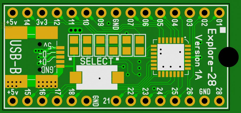
This board was co-developed with robert.rozee, and it was HIS idea. He asked me if I wanted to help with the PCB design. As I love a challenge and knew this one would be a tight-fit, I was all for it - it's all good practise for me. 
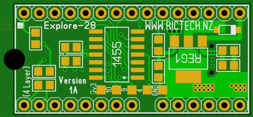
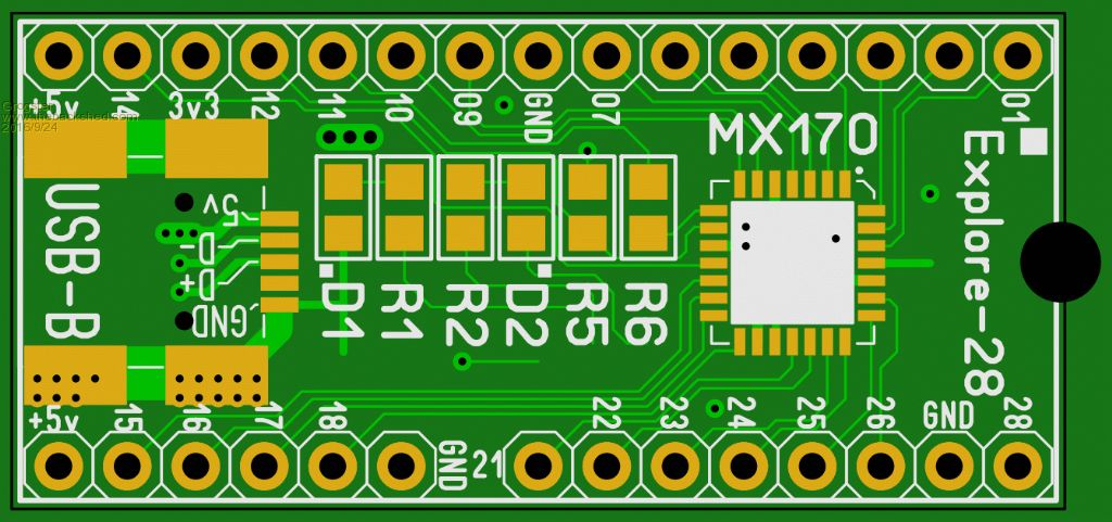
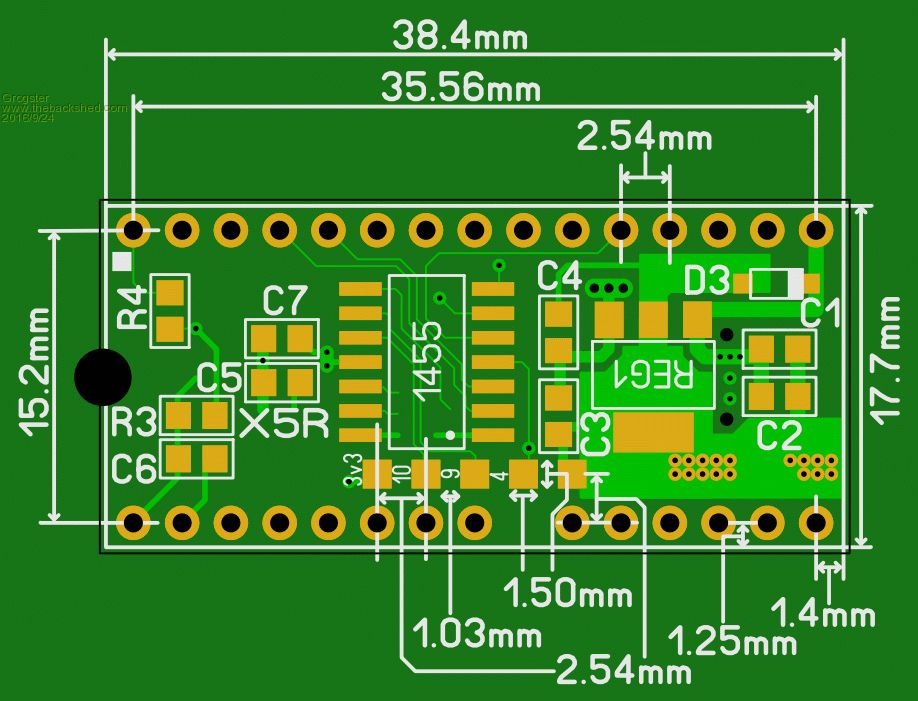
Geoff has approved my use of the "Explore-28" name. What's great about this design, is that you can do away with messy USB-serial adaptors and linking wires, as it is all on-board - just plug in a USB cable. This board uses the 1455 chip for a USB interface and ICSP all via the same USB cable and the ASCII ICSP tool - no need for 100MB+ of Microchip IDE package to get the IPE, and no need for a PICkit-3 either - all programming is done by the 1455 chip and standard USB cable + the free ICSP tool. As you can see from the last image, the board is tiny for what it contains, and is not a great deal bigger then a standard DIL 28-pin chip is. There is a separate dimensions/legend image, as including even the component ID's on the silkscreen made the board look very crowded silkscreen-wise, so we decided to just omit it completely, and have another image with a nice big legend on it. On that image, parts that are on the board that were in the way of the legend were removed from the image - such as the SELECT button. This board uses the PIC32MX170 chip that is at the heart of the Micromite-2, but in the tiny 6mm square QFN package. This chip is PROBABLY not possible to hand-solder without the help of a microscope - 6mm QFN's are not very big! 
The 1455 chip on the bottom is standard SOIC package. Regulator is SOT-223, LED's and the passives are all 0805, and diode on bottom of board is SOD-123. The PCB is four-layer, with the inner layers being used as power and ground in a pretty standard arrangement for four-layer design. Despite the board being four-layer, they work out very cheap on a per-board basis because of their small size - around 50c a board(plus freight), which for four-layer is very cheap. I will be selling boards, kits and assembled modules from my website in due course - the boards have been ordered so should be here in a couple of weeks, and the chips and other parts are also on-order. I have not worked out prices yet for kits and assembled modules, but I will post that here once I have. Smoke makes things work. When the smoke gets out, it stops! |
||||
| matherp Guru Joined: 11/12/2012 Location: United KingdomPosts: 11110 |
Grogster An "improvement" I would like is to use a USB connector with through hole mounting pins. Surface mount connectors are very susceptible to getting pulled off the board complete with the tracks. Surface mount is fine for the pins themselves but the thing is much stronger if the mounts are through hole A version I like is this one |
||||
| Grogster Admin Group Joined: 31/12/2012 Location: New ZealandPosts: 9919 |
You are correct - through-hole would have been better in hindsight. Oh well - maybe for the 1B boards.
Can't say that I have ever managed to do this myself, provided there is plenty of ground copper to solder the case tabs to, then the socket is pretty damn solid, but I do hear what you are saying - if you yanked on the USB cable(perhaps caught it on something), it could pull the whole socket off the PCB ruining it. The trick to preventing that from happening, is - DON'T DO IT!   Smoke makes things work. When the smoke gets out, it stops! |
||||
| MicroBlocks Guru Joined: 12/05/2012 Location: ThailandPosts: 2209 |
I recently remade my module to use the SSOP versions of the chips as the QFN's are a major pain in the .... to solder. Surprisingly using those SSOP did not needed more PCB space as the area under the chips is available for routing. It also allowed for just using 2 layers and all parts on a single side. I also prefer the USB to be through hole as lots of tension is put on it when inserting and removing the connector. After a while they work themselves loose. What you could do is to make the ground pins a lot bigger so the copper pads have a lot more PCB to hold on to. Here is my version (not for sale as i focus on other things now, so please do not see it as competition but an alternative possibility to layout the pcb with SSOP packages!) 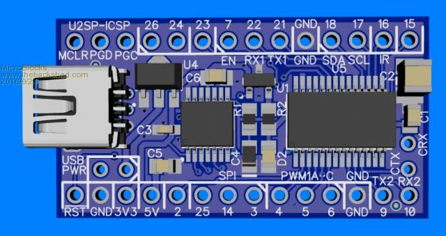
Microblocks. Build with logic. |
||||
| Grogster Admin Group Joined: 31/12/2012 Location: New ZealandPosts: 9919 |
Out of interest, what was such a pain in the posterior when soldering QFN's? Just that they are tiny? Smoke makes things work. When the smoke gets out, it stops! |
||||
| MicroBlocks Guru Joined: 12/05/2012 Location: ThailandPosts: 2209 |
The biggest pain was the amount of solder paste. A little bit too much and you'll have shorts, a little bit not enough and you have unconnected pins. A bit too much on the center pad and you often have one side hovering over the pads without all of them connected. A reflow repeat is a way to fix that, or removing the chip and do it again. Getting them equally heated (center pad and the pins) is another but that can be solved with a good hot plate or oven. After a lot of practice it is better to use a little bit less solder paste on the center pad. Some pcb's i had before that had a solder finish on them could hold the qfn's without adding any solder paste, just some flux. :) Inspecting can only be done really good by using X-ray. Otherwise it is just inspecting with a side view of the pins. A jig to test each connection and a way of determining that there are no shorts between pins is a must. For automated placement/reflow like the professional assembly houses do it is not really a problem. When you need to do them by hand it is way to much time. Hotplate or reflow oven with a good stencil is somewhere in the middle. I have about 450 pcb's left that were made for QFN's. The about 100 i made just took to much time. I got pretty good at it but even then it was too long. In contrast a SSOP is much easier. The amount of solder is less critical, inspection is much easier, placement is easier, fixing a bridge is easier etc.. Microblocks. Build with logic. |
||||
| Grogster Admin Group Joined: 31/12/2012 Location: New ZealandPosts: 9919 |
Ta. Useful information.
I've ordered the boards and chips now anyway(only ten chips for now), and it will give me a chance to play with QFN, which I have not had a chance to play with yet, so it could be a good thing or a bad thing depending on how it goes! Smoke makes things work. When the smoke gets out, it stops! |
||||
| robert.rozee Guru Joined: 31/12/2012 Location: New ZealandPosts: 2498 |
the connection to the centre pad is optional (it is electrically isolated), leaving this out as grogster has done removes many issues. the board is the same footprint as an arduino nano, hence the need for going QFN. the above blue layout looks to be 0.1" wider, yes? cheers, rob :-) |
||||
| MicroBlocks Guru Joined: 12/05/2012 Location: ThailandPosts: 2209 |
The distance between the top and bottom row of pins are 600 mil. Same as a DIP28. The dimension are such that it can be used with a standard DIP28 socket or ZIF socket. Leaving the center pad unconnected can be done but then you loose the thermal connection which leaves only the pins (that are under the chip) to dissipate the heat. A QFN package is specifically designed to dissipate the heat through the center pad. A soldermask and tented vias (and silkscreen) adds an insulating layer that further minimizes the center pad to dissipate heat. It basically renders the center pad useless for its intended purpose. Extra caution will be needed to not stress the chip as specified maximum values in the datasheet will have to be lowered considerably. Another thing to consider is that QFN packages can easily shear off when only the pins are soldered. SSOP or SOIC has a lot bigger pins that can easily dissipate the heat, so no need for a center pad in those packages. There is a small table in the datasheet that specifies the junction to ambient thermal resistance for the different packages. [code] TABLE 29-3: THERMAL PACKAGING CHARACTERISTICS Characteristics Symbol Typical Max. Unit Notes Package Thermal Resistance, 28-pin SSOP �JA 71 � �C/W 1 Package Thermal Resistance, 28-pin SOIC �JA 50 � �C/W 1 Package Thermal Resistance, 28-pin SPDIP �JA 42 � �C/W 1 Package Thermal Resistance, 28-pin QFN �JA 35 � �C/W 1 Package Thermal Resistance, 36-pin VTLA �JA 31 � �C/W 1 Package Thermal Resistance, 44-pin QFN �JA 32 � �C/W 1 Package Thermal Resistance, 44-pin TQFP �JA 45 � �C/W 1 Package Thermal Resistance, 44-pin VTLA �JA 30 � �C/W 1 Note 1: Junction to ambient thermal resistance, Theta-JA (�JA) numbers are achieved by package simulations [/code] The values for a QFN are considerably lower. And those numbers are for a connected center pad. The biggest impact on that number in the case of a QFN is how the PCB is designed with regards to the center pad, how many layers, vias etc. This is considered the biggest influence. JEDEC specifies exactly how these values have to be measured and the way it is mounted on the pcb is considered as a 100% effect on the results. Microblocks. Build with logic. |
||||
f1fco Senior Member Joined: 18/03/2012 Location: FrancePosts: 155 |
hello Grogster, Explore 28 not yet on your site ? I am interested by 2 pieces... Pierre, from Nimes, south of France 73s de F1FCO |
||||
bigmik Guru Joined: 20/06/2011 Location: AustraliaPosts: 2979 |
GDay Rob, Doing a Photoshop resize to do a comparison it appears that Grogster's board and Jean's board are the same height with a 0.6" pin spacing, but Jeans board has a bit more PCB substrate top and bottom making the PCB itself 0.05" higher. With the Width measurement Grogster's is 0.1" wider than Jean's board.. Not that this is a `mine is bigger than yours' comparison.. Just interesting that two almost identical boards are out there.. @Jean, Why are you not going to release your board? IMHO it will be a heck of a lot easier for silly old buggers like me to solder the SSOP chip than the QFN. Kind Regards, Mick Mick's uMite Stuff can be found >>> HERE (Kindly hosted by Dontronics) <<< |
||||
TassyJim Guru Joined: 07/08/2011 Location: AustraliaPosts: 6497 |
Grog's board is 30 pin. I think you would need to use 32 pin sockets but that's no big deal. I like Grog's pinout - the same as the 28 pin DIL chip with the 5V added at the end. My own version made on my CNC will end up about 4 times the size. Jim VK7JH MMedit |
||||
| Grogster Admin Group Joined: 31/12/2012 Location: New ZealandPosts: 9919 |
Hey folks.
Thanks for all the comments. QFN's have been ordered, so IF there is an SSOP version of this, it will be a 1B. Personally, I don't really see heat as being a major issue with the MM2. The chip itself sucks about 30mA, so that is no problem, becasue there is no significant heat from that. If you are worried about the combined sink/source current of the I/O pins added into the mix, I also don't really think this will be that much of a problem - we'd have to build a few and see what happens. At the end of the day, you should really be using buffers on any I/O pin that needs to sink or source more then a couple of mA - IMHO only. I also don't REALLY see how they could be that easy to shear-off with only the pads holding them there. Provided you are not drop-kicking the module around the workshop, or chiselling at it with a screwdriver that should never be any issue at all. Not saying it can't happen, just don't really see how that is going to be that much of a problem. Having said all that, a blob of silicone-sealer over the chip or spread around the edges would effectively glue it down, but I don't see the need. I DO hear what you are saying Jean, but I really don't see these as being THAT much of a problem enough to prevent me using the QFN. It remains to be seen if I am wrong on that one, but we'll find out soon enough!
@ f1fco - No, not on website yet, as I don't actually have them here to sell - yet. Parts ordered, but I will need to wait for their arrival before I list this one on the website. Smoke makes things work. When the smoke gets out, it stops! |
||||
| robert.rozee Guru Joined: 31/12/2012 Location: New ZealandPosts: 2498 |
i've been doing a bit of research, and dug up the following datasheet from maxim: http://pdfserv.maximintegrated.com/en/an/AN862.pdf according to Table 2 (page 8): Thermal Resistance Example ----------------------+----------- Board Configuration | theta JA ----------------------+----------- Unconnected EP | 39.91 Soldered EP | Large Board | 19.09 Small Board | 28.14 the point of interest is the difference between 19.09 and 39.91 (with/without the thermal pad soldered). these numbers suggest that even in the absolute worst case, an isolated thermal pad will result in QFN thermal performance approximately equal to that of an SSOP. and how many folks have had a micromite getting even slightly warm in normal operation? cheers, rob :-) |
||||
| MicroBlocks Guru Joined: 12/05/2012 Location: ThailandPosts: 2209 |
The whole document explains the use and at the end it has that table and right after that table in that specific document it says: [quote] ...seen from these experiments, proper use of the exposed paddle greatly improved the performance of the device. Incorrect use of the exposed paddle can lead to increased failure rate, decreased electrical performance or permanent thermal damage. Board size and proper soldering of the exposed paddle were shown to have a large effect on the overall thermal performance. 6 Summary The exposed paddle greatly improves system level performance by increasing thermal dissipation, decreasing workable package size, and improving electrical performance. Proper soldering of the exposed paddle to a suitable thermally conductive surface, such as a ground plane, is critical in obtaining the improved performance of the exposed paddle package and proper operation of the IC. [/quote] Bold words are to emphasize the pretty strong words that are used. Should i just ignore those? Microblocks. Build with logic. |
||||
| Nathan Regular Member Joined: 10/01/2016 Location: GermanyPosts: 49 |
Hi MicroBlocks, I fully agree with your understanding. ;-) QFN can be handeled very well in case professional equipment for soldering is available and radian control is available, too (automotive). For home use it is a nightmare. The center bump is extremeley important for temperature control. In some situations also for distribution of VSS to the core chip. Also for stability of the package it is better to solder it. So if possible I try to avoid it. Sometimes for some sensors it is impossible. Nevertheless follow your feeling. Risk reduction is a very good strategy. (remember my default pin discussions) Do not run in the same trap. Have fun, Nathan |
||||
| robert.rozee Guru Joined: 31/12/2012 Location: New ZealandPosts: 2498 |
the numbers speak for themselves: an isolated thermal pad will result in QFN thermal performance approximately equal to that of an SSOP. the QFN package was designed to provide superior thermal performance for higher-power devices when the thermal pad is soldered to a PCB. the mx170 is not a higher-power device; while one can solder the thermal pad if desired, the numeric data suggests this will have no material benefit at the power dissipation levels at which a micromite/mx170 typically operates. cheers, rob :-) |
||||
| Grogster Admin Group Joined: 31/12/2012 Location: New ZealandPosts: 9919 |
I'm inclined to agree with Rob on this one, guys. I do certainly hear what you are saying about the thermal pad for both thermal and physical restraint reasons, but in this particular case, I don't think there will be a problem. I will build one that I will torture-test with reasonably heavy loads on all it's I/O pins at once to see what happens. Generally speaking though, if you are driving relays, you use a transistor buffer. If you are driving an LCD, it is only microamps of current per I/O pin to the controller on the LCD itself. YES - if you loaded up the module I/O pins with 15mA or so in source or sink all at the same time, we might have a problem, but we'll see what happens with the 1A, and if it DOES prove to be the massive problem some are suggesting that it will be, we can change the design for the 1B's. The 1A's of any board I do are technically the prototype run anyway.
It's going to be interesting whatever the case, but if it proves to be a problem, then I will allow MicroBlocks etc to publicly say: "I told you so." Smoke makes things work. When the smoke gets out, it stops! |
||||
| MicroBlocks Guru Joined: 12/05/2012 Location: ThailandPosts: 2209 |
Well, at least i told you so that you are aware of it. :) Lots of details are hidden in datasheets and are not obvious. The datasheet only shows numbers when the center pad is soldered. There are no numbers for when it is left unsoldered. Therefore there can be no useful estimate of how it will function. Using another manufacturers document of a totally different chip says absolutely nothing because it is all about how the die is placed and what measures where taken to direct the heat to the pad in this particular chip. The reason for my first post was to actually show that using SSOP does not really use that more room then a QFN and are therefore a good candidate for small pcb's. This was pointed out to me by another member and i thought it could not be done. I have since then changed four designs i had with QFN's to use SSOP instead and all four of them where possible. That experience of adapting the design and the fact that SSOP packages are much easier to solder made them my preferred package. It is also good to at some time commit to a certain package as it would then be easier having them in stock. I now have some chips in three different packages, of which two will probably never be used. Wasted money and wasted time. Microblocks. Build with logic. |
||||
| robert.rozee Guru Joined: 31/12/2012 Location: New ZealandPosts: 2498 |
actual hardware, assembled and running: 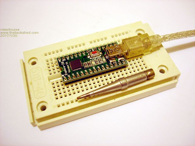 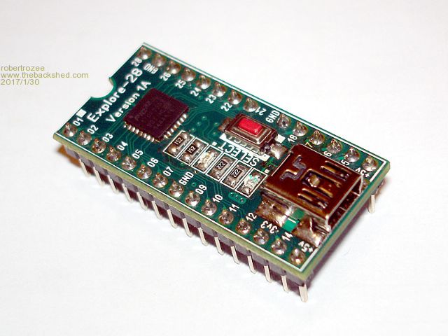 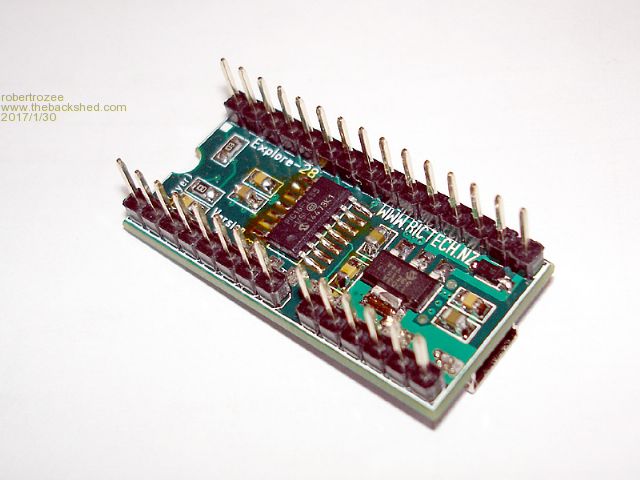 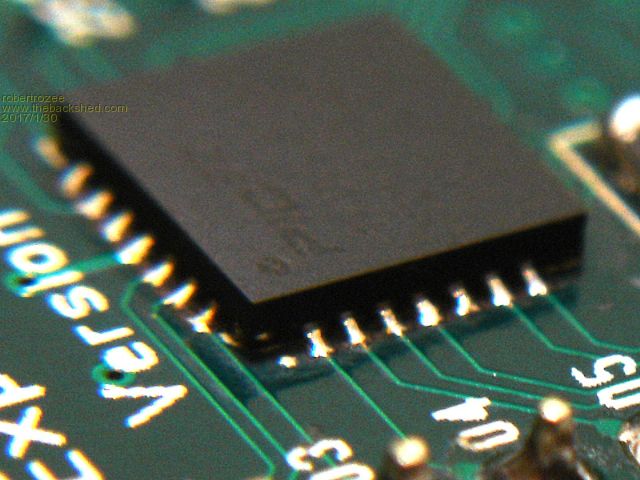 cheers, rob :-) |
||||
| Page 1 of 3 |
|||||
| The Back Shed's forum code is written, and hosted, in Australia. | © JAQ Software 2026 |
