
|
|
Forum Index : Electronics : 100 Volt Modular H-Bridge Designs
| Page 1 of 3 |
|||||
| Author | Message | ||||
| Solar Mike Guru Joined: 08/02/2015 Location: New ZealandPosts: 1228 |
Starting this new topic as a record of various H-Bridge designs I want to experiment with; all comments are welcome including criticisms, we are here to learn. Its been a long time since I played with this so have bound to have forgotten a few things. Currently I'm converting my home system to 100v operation; reasons being I want to run some welders, air compressors, the house including the electric stove. Some of the peak loadings will be quite high and perhaps requires a re-think of previous attempts to get it all working. With the high loads, I figured the higher the DC voltage the better, by splitting up the existing 16 pairs of Lifepo4 batteries into a 32 series string, this will give me nominal 100v system varying between 96 and 112v. I want to make the H-Bridge power mosfet stages modular; by this I mean splitting up the Bridge into two half bridge pcb's that are linked together. If higher output power is required then another set of boards can be paralleled with the existing, all driven from the same driver. Here is the first attempt, the 1/2 bridge pcb 162 x 113mm has 6 mosfets, these are arranged under the pcb and clamped by it to the 5mm alloy side panel of the case, now acting as a heatsink. A 100 x 100mm capacitor board bolts across the top; I have an assortment of caps here and its easier to use them all up by changing the cap board and not having to re-design the main one. Each mosfet has its own driver chip, the UCC27511A has a split output with a 8amp sink current, so should work quite well in preventing the Upper stage turning the lower mosfet on due to its miller capacitance and fast dv\dt transitions. Each set of three are driven by a simulated opto-isolated driver and have their own 12V supply. All upper and lower "Grounds" are star connected so there can be no induced voltages or ground bounce stuffing up the drivers. For 100v operation pcb traces will be good for > 100 amps using 2oz copper, 48v copper bars can be placed on the pcb to increase current capacity. For my system I will be using 3 sets of boards in parallel, I think 300 amps @100v will be enough. Top 1/2 Bridge: (2 required for full bridge) 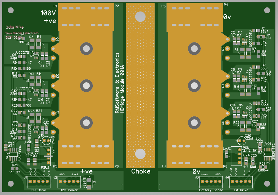 Bottom: 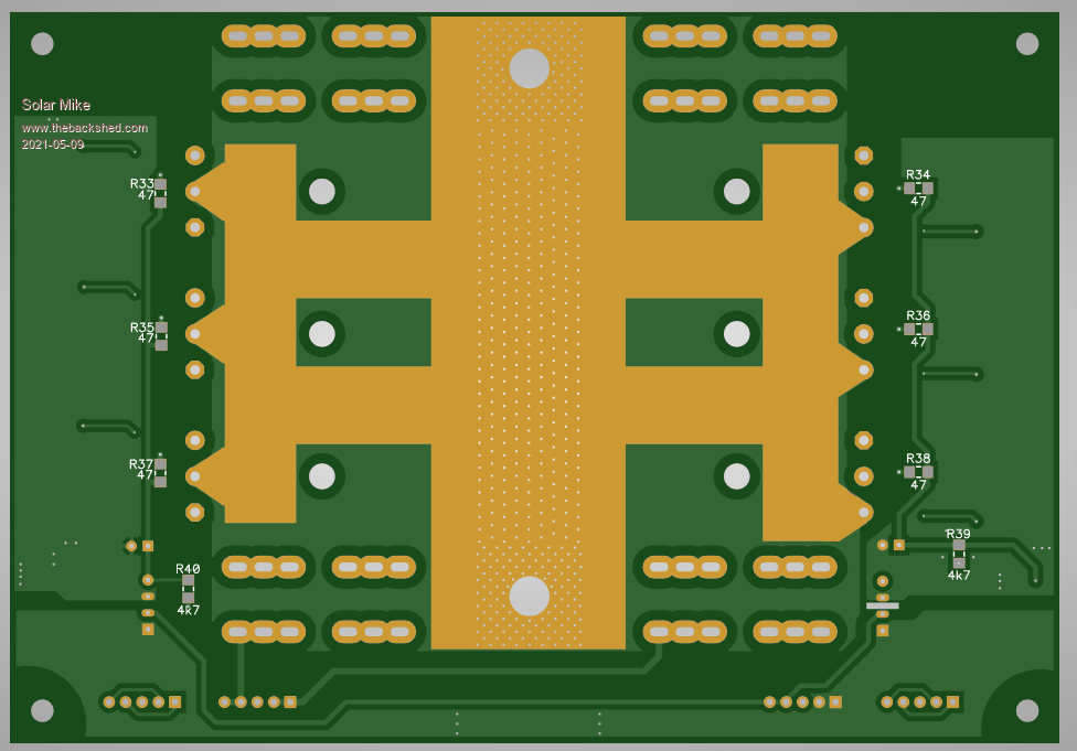 Already I can see an error, will post the Cap pcb next, it bolts across the top, with 4 connection points for each power rail, then draw up the schematic showing how they can be combined. Cheers Mike |
||||
| Warpspeed Guru Joined: 09/08/2007 Location: AustraliaPosts: 4406 |
I have been running a 100v system now for over three years. Originally it terrified me, but after three years, have had full body contact direct across 100v dc many times, and never felt even a tingle. Mosfet technology has come a very long way, and now there are some pretty good high voltage low Rds-on mosfets around, that did not exist a few years back, so this all makes a great deal of sense. The reduction in dc current is a huge advantage in every respect, and you will gain everywhere. Only disadvantage will be the larger number of battery cells that need monitoring, but that is not a big issue. I no longer have much personal interest in high frequency PWM, but it still has a lot of applications. If pursuing very high power, I think the best way forward might be the modular approach, using multiples of proven half bridge power module designs each operating individually feeding the transformer through individual chokes. I cannot recall who came up with this idea (its not mine) but its brilliant  The individual modules and chokes do not have to switch in phase at 20Khz, in fact there would be advantages in PWM ripple cancellation of they were deliberately switched out of phase. I will follow Mikes progress with great interest, I believe this is the next big step forward for all of us. Cheers, �Tony. |
||||
| Solar Mike Guru Joined: 08/02/2015 Location: New ZealandPosts: 1228 |
Wiseguy-Mike gave me the idea, so credit goes to him for suggesting it. The board above could be simplified by using less mosfets and perhaps having a single isolated driver chip for each Upper and lower halves; then using greater numbers of modules connected in parallel to get the required output power, the chokes would then be much smaller. I have suggested 3 mosfets to share the 100A RMS in my design as if any single device is faster or slower than the others, it could probably handle the full 100 amps for a microsecond until the others started sharing, having individual drivers would allow increasing PWM to a higher frequency, say 50Khz, the chokes could then be much smaller powdered iron cores. I will be using two chokes per set of two boards, so 6 chokes in all; have yet to sort out a readily available off the shelf bare core for these that wont saturate @100 amps. Not sure Warp about the out of phase bit, the SPWM's surely must be in phase if they were all driving a single large toroidal core. Out of phase would work in a buck converter, not here.?? Cheers Mike |
||||
Haxby Guru Joined: 07/07/2008 Location: AustraliaPosts: 426 |
Looks good to me. A few of these could be used for a warpverter style build too. I'm guessing you will be using screw type connectors to link the capacitor board? Without doing the math, I'd suggest more capacitance at the gate driver ICs. I only see 1uf and 0.1uf |
||||
| InPhase Senior Member Joined: 15/12/2020 Location: United StatesPosts: 178 |
I think he meant just out of phase enough for one waveform to fill in the ripples of another. A degree or two maybe. |
||||
| Solar Mike Guru Joined: 08/02/2015 Location: New ZealandPosts: 1228 |
Its a pretty generic design, so could have other uses, I wanted to make a high power device that didn't result in an "Engineering Project" of complex metal work, there is scope to add copper bars in the tinned areas for greater current capability, sorry about the smd stuff, its all I use now as its difficult to get suitable active devices in PDip now. 4mm bolts pcb screw connectors used. Will check the math on driver caps, note 12v psu with 22uf electro supplying each bank of mosfets, no bootstrap here, so caps can be quite small. Cap PCB 100x100mm: 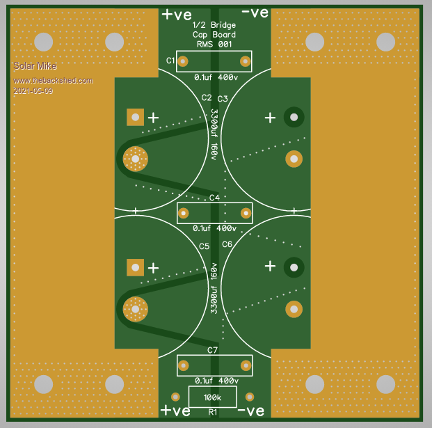 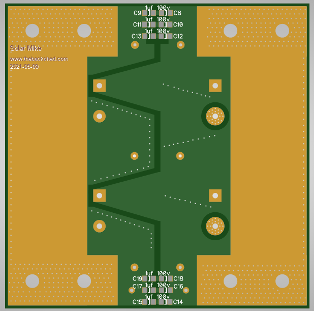 Cheers Mike Edited 2021-05-09 21:47 by Solar Mike |
||||
| nickskethisniks Guru Joined: 17/10/2017 Location: BelgiumPosts: 481 |
Ok, just throwing some ideas: I was thinking about something similar to design, but I'm (was) stuck a bit, you gave me new ideas with this. I think it's good to have gate driver and power part separated. And I'm very curious if a dedicated gate driver for each mosfet is worth the trouble and extra money. I think I want to copy you idea just to test if that's ok. Why did you choose to put the choke connection also on the top pcb? Wouldn't you be able to make your connection with your choke on the bottom? Ok, you create a thicker choke layer and wider + / - track and have place for the screw terminals with your way, but you could solder/bolt a copper piece on it too. You could also put the bypass capacitors on the top plane of the mosfet board that way. You probably need to add some alu/copper piece under the mosfets to increase the distance between the pcb and heatsink. You can try to put your bypass capacitors on the mosfet board, closest to your mosfets you can. If using big enough or axial capacitors they fit over the choke connection. But probably too high to fit under the capacitor board with the screw terminals and maybe make no difference. You can try to use brass studs to make the connection between the capacitor board and the mosfet board. With those you can also hold the mosfets in place and create space for the 100n and 1uF caps, you can widen the mosfet hole to 4mm. Something like this: (the yellow thing should present the capacitor board. The pp capacitors could be replaced by ceramic to safe space, the PCB could be inforced with busbars) 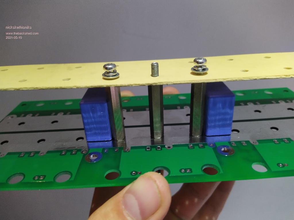 Pictures are just for a 3D view to give an idea, I know there is a short this way, isolation of separate potentials could be an issue and must carefully considered. The bolts could be sinked in to an aluminium bar under the mosfets, MOSFETs should be isolated with thermal pads. The bar could be mounted with other bolts to the heatsink, but should also be isolated because it is carrying a potential because of the bolt. 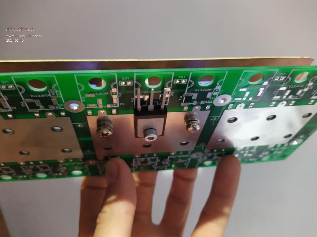 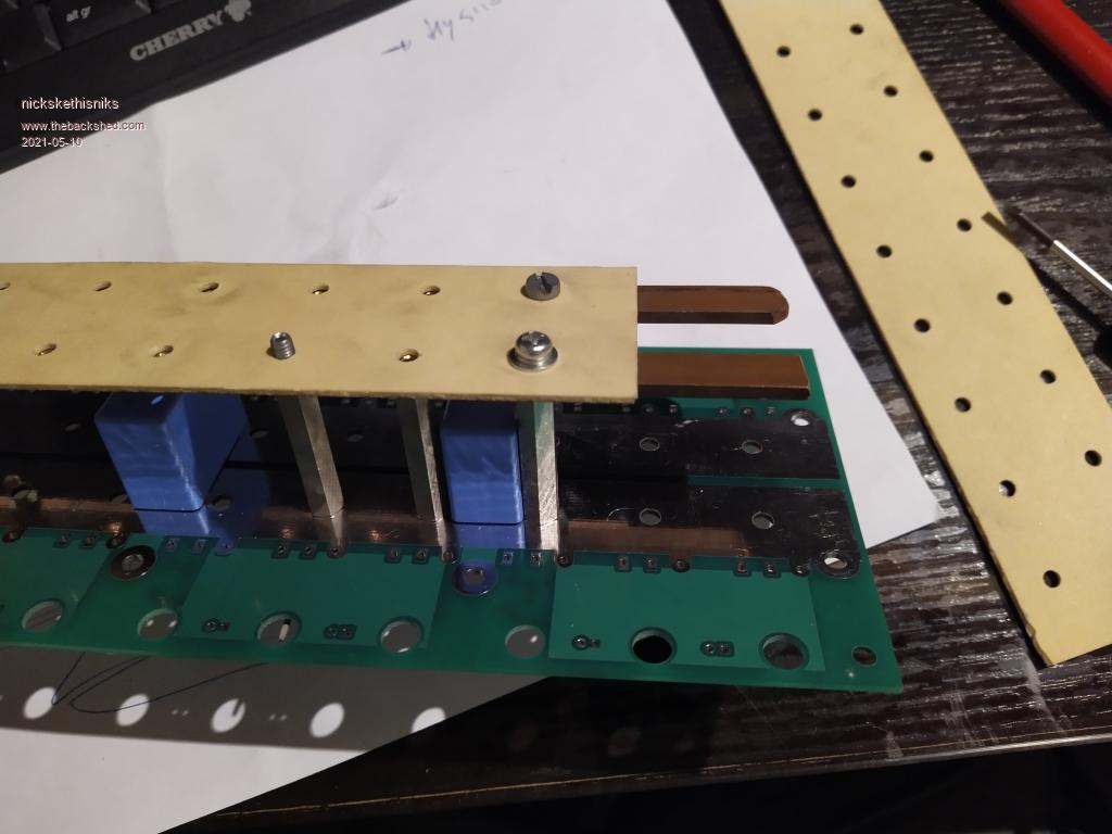 Edited 2021-05-10 08:05 by nickskethisniks |
||||
| Haxby Guru Joined: 07/07/2008 Location: AustraliaPosts: 426 |
Solar Mike, do you do any signal conditioning, low pass filtering or anything to the logic pins coming out of the nano? Or do the nano pins breakout straight to the emulated optocoupler MOSFET board above without anything in between? |
||||
| Haxby Guru Joined: 07/07/2008 Location: AustraliaPosts: 426 |
And if no filtering, what distance would you say would be ok to run the wires? |
||||
| Solar Mike Guru Joined: 08/02/2015 Location: New ZealandPosts: 1228 |
Copy away. Dedicated driver is a best case scenario, keeps the nH inductances in the gate circuits down to a minimum, low inductance means full gate charge can be applied to each mosfet quickly with less ringing, miller effect dv\dt unwanted turn on is also reduced as the gate driver shunt resistance is much closer resulting in faster clamping of unwanted events. Extra costs for the drivers, what $30 for a set of 2 boards, isnt really an issue... Having multiple mosfets off a single driver obviously works as that's what a lot of DIY designs do, not so much in professional designs though, depends on what you think you can get away with and how fast they must be turned on\off. I would like to try 50 Khz spwm, so design gets more critical. Choke copper bar if used, was placed on top as it wouldn't fit under the board without lengthening the mosfet leads, longer leads = more inductance. But you raise a good point with the positioning of the bypass caps, so I have made some modifications to both boards and placed the bypass ceramics on the main pcb and removed the choke bar from the top. I wont be actually using any additional copper bars as the 2oz copper tracks are sufficient for > 100 amps odd. If a copper bar is required the mosfets can have a spacer piece between them and the heatsink, same thickness as the bar, so their short lead length isn't compromised; want to keep the "Engineering" metal work to a minimum. Brass isn't a particularly good conductor, the copper pcb screw terminal standoffs for the cap board are 6mm height, again I want those lead lengths with high currents in them minimized. Spacing the cap pcb higher up isnt the best option here. Thought of using the 5mm gold flashed brass push fit terminals the RC guys use for heavy battery currents and soldering to the pcb, have a heap of them here as I use them for making power test leads etc, the 5mm ones can each handle 50 amps without getting warm, they take up little room so more could be used. Main PCB Ver 002: 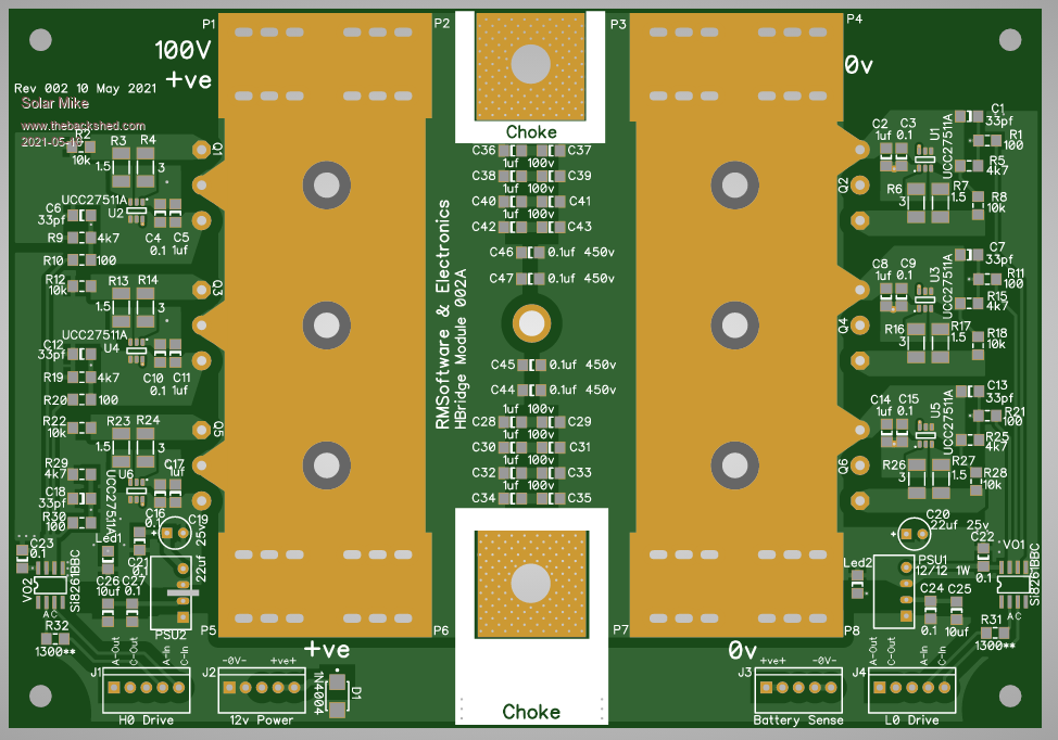 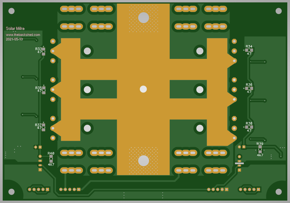 Cap PCB Ver 002: 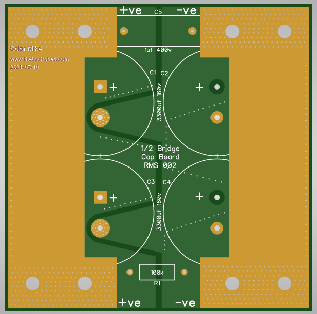  Cheers Mike |
||||
| Solar Mike Guru Joined: 08/02/2015 Location: New ZealandPosts: 1228 |
Was going to use Poida's nano driver, once its sorted, it uses two IR2184 1/2 Bridge drivers to create the required full bridge 12v drive signals with dead time etc. Intention is to use a twisted pair cable to each isolated driver, single resister on each pair is required to set drive current to 8 - 10 mA. The emulated drivers are pretty immune to interference, as there will be no earth or grounds in the circuit. Will it work, should, been ok on other projects using the same or similar drivers; Distance: don't know, could always use shielded micro-phone cable. The individual mosfet drivers have a 100r resistor and a 33-100pf cap at their inputs to get rid of RF hash, so they should be ok. As I'm not using any boot strapping, 1uf which is about 10x the mosfets input capacitance should be fine. Edit: Emulated Opto drivers, the ones I'm using and others only have a reverse voltage into the opto part of 0.3 volts, so you cannot power two of them from a push\pull logic driver in anti-phase to prevent shoot thru. However the latest Texas Instruments UCC23513 simulated opto driver has a 14v reverse input voltage, so it can be used from a push pull source. Copper Bars: AliExpress have an assortment, I have ordered some of These 15 x 3mm, not for the pcb but for battery links between cells in a small 24V 200AH bank, they will fit on the pcbs if required. I have found the best source for copper sheet is a roofer who uses rolls of the stuff to make copper spouting's, normally half hard 0.7mm thick, they have it in their scrap bin. Cheers Mike Edited 2021-05-10 18:04 by Solar Mike |
||||
| Solar Mike Guru Joined: 08/02/2015 Location: New ZealandPosts: 1228 |
Schematics: 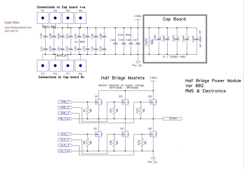 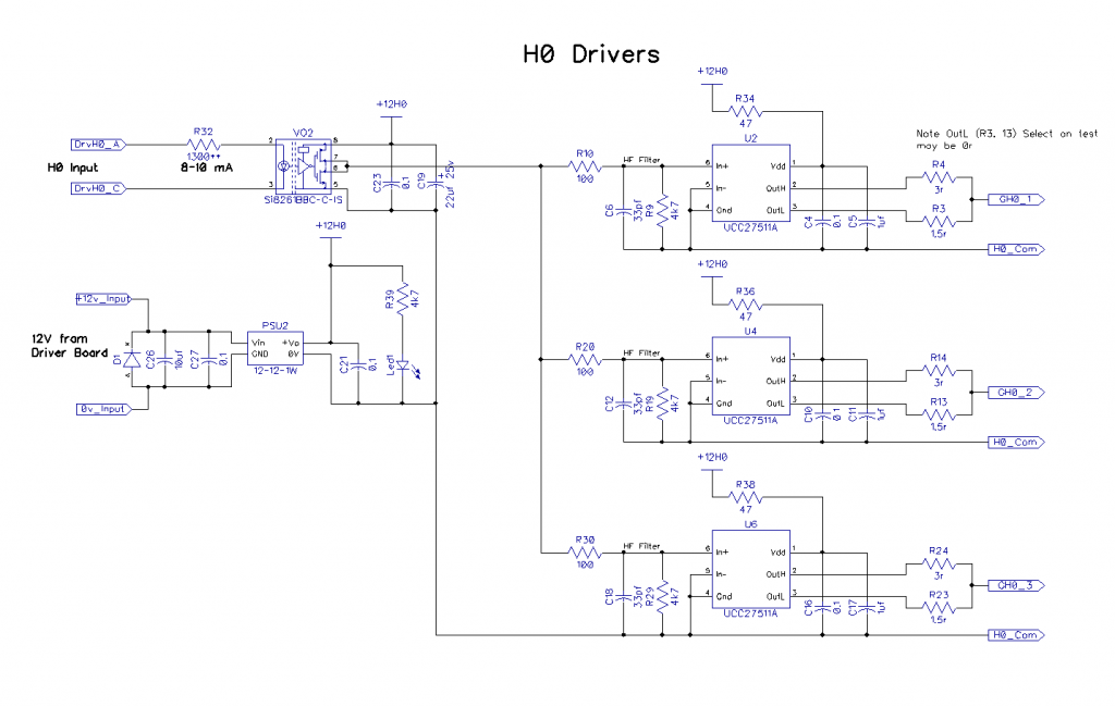 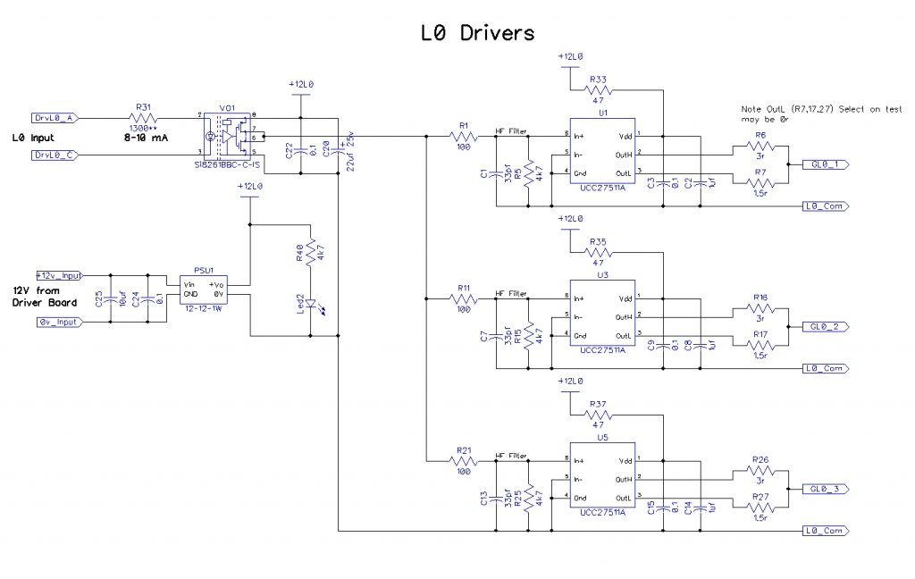 Note: The mosfet drivers have TTL level CMOS compatible inputs, but they can tolerate full mosfet bias drive voltage, so will be ok driven from the Isolator driver with its rail\rail 12v output. Question will be asked why don't you use isolated drivers here and do away with the input driver chip, yes would work, comes down to cost, the little 6 pin non-isolated drivers cost 1/3 of the main input one and there are a lot of them. I haven't shown the 5pin spring loaded input sockets in the drawing, its pretty clear on the pcb where they connect to, there are extra connections on them to allow a daisy chain wiring to another parallel board. Obviously to make a full bridge we need another 1/2 Bridge set of boards, I will draw a block dia showing how multiple parallel sets of modules are connected. Cheers Mike Edited 2021-05-10 22:24 by Solar Mike |
||||
| Warpspeed Guru Joined: 09/08/2007 Location: AustraliaPosts: 4406 |
Anyone in Australia looking for a good source of copper, George White is a family owned business located in Melbourne and Sydney that sell all forms of copper, sheet, bar, tube etc... Looking really good there Mike Cheers, �Tony. |
||||
| Solar Mike Guru Joined: 08/02/2015 Location: New ZealandPosts: 1228 |
Wiseguy suggested this method to me for joining up a number of lower powered H-Bridges in order to better share the total current more evenly through all mosfets. I think its a great idea and should allow better reliability in getting higher output power. At the extreme one could build a single H-Bridge with 4 mosfets and 2 High\Low driver chips per bridge and combine them together to get whatever power output is wanted. The only down side is getting suitable repeatable chokes, probably not second hand and higher costs in all the parts. I will be using 6 modules each with a nominal 100 amp capability. Have yet to do some testing on powdered iron ring cores to make the 6 chokes. Here is a proposed block dia to connect them together. 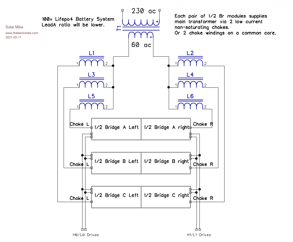 Cheers Mike |
||||
| Warpspeed Guru Joined: 09/08/2007 Location: AustraliaPosts: 4406 |
Chokes will not be at all critical, its just a series impedance, negligible at 50Hz, considerable at 20Khz. This paralleling is done all the time in higher powered radio transmitters, and for similar reasons. Nice tight layout with a small number of power devices per module. Cheers, �Tony. |
||||
| wiseguy Guru Joined: 21/06/2018 Location: AustraliaPosts: 1297 |
I have thought more about the method and I'll ask for Warps thoughts on this too. The 3 chokes on one side should/might be able to share one common (larger of course) choke with paralleled turns. If the turns are chosen to be a multiple of 3, say 12 strands for instance. Then the equivalent of the 3 chokes could be formed by grouping 3 lots of 4 strands. I'm sure the fist thoughts will be that its a crazy idea, but we are not winding a transformer to transfer energy to another winding we are storing an additive magnetic field in the choke windings. Although untested/unproven as yet I believe (think) there will only be minor transformation between the groups of 4 wires for adjacent modules. I'm confident/wondering that in any event it should perform much better than the hard wired paralleled FETs with their current sharing and ton/off issues, and construction & wiring should be less complicated. Exploring options and tossing ideas out there....... Edited 2021-05-11 17:00 by wiseguy If at first you dont succeed, I suggest you avoid sky diving.... Cheers Mike |
||||
| Solar Mike Guru Joined: 08/02/2015 Location: New ZealandPosts: 1228 |
The individual chokes on each side are all switched concurrently in phase, so they are effectively all in parallel with each other. Replacing that combination with a single larger core and 3 sets of phased windings seems exactly the same to me, they are still in parallel and the currents are shared. A large core may be easier to get from a junked inverter, perhaps more difficult to wind. Mike |
||||
| Warpspeed Guru Joined: 09/08/2007 Location: AustraliaPosts: 4406 |
I agree Mike, its a great idea with a lot of potential. Provided the inductance is sufficient to reduce ripple current to a low proportion of the 50Hz main bulk current, you don't need to use any special wire, or even a high frequency core. Skin effect and core losses will be negligible because both are magnetic effects produced by current (not by voltage). So steel or powdered iron core and solid wire will work fine because the bulk of the current is only swinging smoothly up and down at 50Hz. Any small residual ripple at 20Khz should be very low in comparison, and the evils of high frequency loss will also be so minor, we can safely ignore them. That assumes there is enough inductance to reduce the high frequency ripple sufficiently, which is not too difficult. We have to do that anyway, because the main output toroid uses a steel core and solid wire, and both are in series and see the exact same current. The function of the choke is to reduce high frequency ripple. Once that is achieved, both choke and toroid only need to be built to work well at 50Hz. Edited 2021-05-11 17:39 by Warpspeed Cheers, �Tony. |
||||
| nickskethisniks Guru Joined: 17/10/2017 Location: BelgiumPosts: 481 |
Wiseguy, something like they do when you want big switching paralleled thyristors to share the current? Edited 2021-05-11 20:22 by nickskethisniks |
||||
| wiseguy Guru Joined: 21/06/2018 Location: AustraliaPosts: 1297 |
Sorry Nicks - I have never had the pleasure of working with high powered paralleled thyristors. I have worked with a few 3phase multiple single water cooled semikron thyristors in a 12 pole rectifier that handled 2000A total @ 125VDC but thats my biggest. I am aware that it is common to have an inductor even with single thyistors - I thought that was for moderating/controlling dvdt issues. I just went out to the back shed.... and I found a baby shunt & cable only 750A!  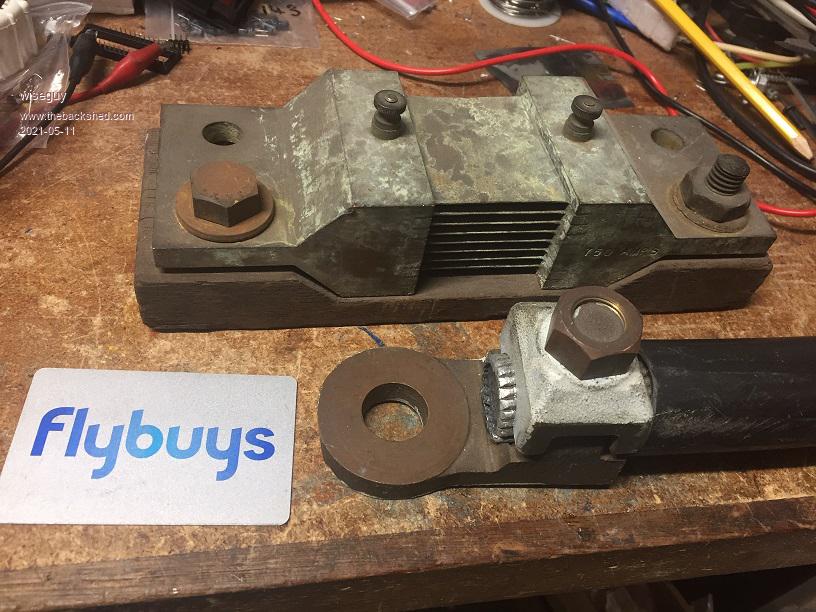 If at first you dont succeed, I suggest you avoid sky diving.... Cheers Mike |
||||
| Page 1 of 3 |
|||||
| The Back Shed's forum code is written, and hosted, in Australia. | © JAQ Software 2026 |
