
|
|
Forum Index : Electronics : Yet another charge controller
| Author | Message | ||||
powerednut Senior Member Joined: 09/12/2009 Location: AustraliaPosts: 221 |
It seems to be the season to design and build your own charge controller, so I'm joining in the fun with my current project. I'm working on a modular design, with a central microcontroller (AVR, but PIC or PICAXE should work fine with minor modifications), and seperate modules for each power source. The modules are responsible for handling the heavy-current switching (connect source to battery, connect to dump1, connect to dump2), providing a sample voltage and current back to the microcontroller board). The microcontroller board will have up to 2 seperate 10-bit ADCs, each of which can handle the both inputs for 4 source modules and transfer data back to the micro via the SPI bus. The microcontroller board also has a Real Time Clock chip (also SPI, hopefully), SD card slot (for datalogging, also SPI) and a 2 line LCD display, plus 3 input buttons and a reset button and some indicator LEDs. All the various inputs and outputs overwhelm the little atmega168p that I've selected as the main processor, so I'm using shift registers (74HC595N) to get the required number of outputs. This makes it damn easy to expand and add more inputs and ADCs if necessary. Finally there is a 4.096V precision voltage reference for the ADCs. finally there will be a power supply board, which will supply the 5V and 3.3V to the modules and main board. Being an electronics noob this will probably take me a while to design and put right, no doubt with many interations of the magic smoke escaping and then the wait-for-replacements. Fortunately Gizmo and <not sure, Gizmo again?> have been kind enough to publish both the PicAxe based charge controller and the PicLog so I have some really nice reference material to ahh.. borrow. I intend to return the favour and "open source" mine, if I get it working correctly. Oh... the reason for the multiple sources is I want to play with some homebrew MPPT stuff next, and I want to be able to test and log both the MPPT'd output and the control output (2 identical solar panels) without screwing with my existing solar and wind setups. Plus I'm going to add more wind/solar to the system later, and it'll be a lot easier to just build a new source module for each thing I add, than to rebuild the whole system to cope with the higher-than-designed-for amperage. Comments and suggestions would be appreciated. |
||||
| Gizmo Admin Group Joined: 05/06/2004 Location: AustraliaPosts: 5185 |
Hi powerednut Sounds like a big project for a electronics noob, but I'm guessing you've built a few projects before. Building the charge controller in modules is a good idea, that way you can take you time with each section, sorting out the bugs as you go. Having two idential solar panels side by side is a good idea if your going to play around with MPPT. Glenn The best time to plant a tree was twenty years ago, the second best time is right now. JAQ |
||||
| powerednut Senior Member Joined: 09/12/2009 Location: AustraliaPosts: 221 |
Thanks Glenn, I've built a few things before, but this is only my 5th time designing something from scratch. There is an awful lot I still don't understand, but its a fun way to learn. Smelly sometimes though. Nothing like the smell of burnt silicon. My last little design project was a simplified charger. No LCD, the ADC was handled by the micro, only one source, and no load dump as it was a solar charger. No logging either. It worked okay, but was a pain in the neck to calibrate and debug. I learnt a lot from it though. Anyway question time: I'm trying to decide on the best current sensors to use. I'm having trouble deciding if its better to use a closed loop sensor like a ACS756SCA (100A, datasheet, about $7.20 a pop from digikey) or an open loop sensor like a FHS 40-P/SP600 (also 100A, datasheet, about $4.90 each from digikey ). The closed loop sensor incorporates the shunt resistor, so its pretty much a drop in part. The open loop sensor doesn't need the shut resistor, and can either be mounted over the +V track, or under the cable. I'm currently leaning towards the closed loop sensor, because it seems simpler to me. Am I wrong?, would it be better to use the open loop sensor? Any suggestions for alternative solutions? |
||||
| powerednut Senior Member Joined: 09/12/2009 Location: AustraliaPosts: 221 |
Okay, slow progress, but here is the first attempt at a Solar charger module. I've not used Mosfets in this particular configuration before (copied it from Gizmo's circuit) and it is untested at this point as I'm waiting till I have everything designed before I put in a parts order. Build at your own risk. PCB layout to follow once I know it works. It should (I hope) work fine for 12V or 24V systems with no changes. Higher voltage systems will require a few changes. The voltage divider (R1, R2 and TR1) should output a voltage somewhere in the range 0-4.096V. For the 12V and 24V systems, as drawn, it should output 1/10th the input voltage(i.e 1.2V for 12V). The resistors i've specified for 48V systems should output 1/20th (i.e 2.4V for 48V) when adjusted with TR1. Parts are available from digikey. 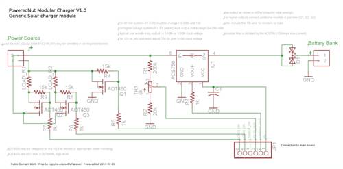
Comments and suggestions welcome. |
||||
| powerednut Senior Member Joined: 09/12/2009 Location: AustraliaPosts: 221 |
Here is the generic wind turbine charger module. Pretty much identical to the solar, with a minor redraw for clarity and the addition of the rectifier. same details as before - it has not been experimented with, built or tested. use at own risk. 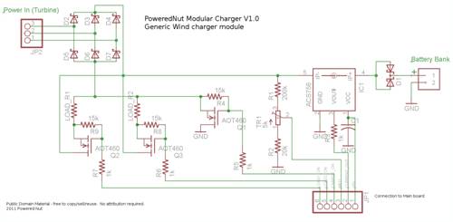
Comments and suggestions welcome, as before. |
||||
Downwind Guru Joined: 09/09/2009 Location: AustraliaPosts: 2333 |
Hi, Can you put the schematics in a pdf file and upload the file as i can not read them and the blur to much when i enlarge them. curious..........why the diodes across the battery, they just create further losses. Pete. Sometimes it just works |
||||
| Tinker Guru Joined: 07/11/2007 Location: AustraliaPosts: 1904 |
Even more curious is the diodes (at the positive battery terminal) are drawn as zener diodes. Forward biased zener diodes are supposed to do what??? Klaus |
||||
| powerednut Senior Member Joined: 09/12/2009 Location: AustraliaPosts: 221 |
umm.. they are low resistance schottky diodes actually. The part number got dropped for some reason. That particular part contains two diodes, which comes up in eaglecad like that. The diodes were there to prevent the battery discharging back through this circuit - though the voltage divider wont produce much drain. I wasn't sure what the best way to calculate the loss of power from the diodes was, in comparision to loss through the divider. PDFs coming up. |
||||
| powerednut Senior Member Joined: 09/12/2009 Location: AustraliaPosts: 221 |
PDFs as requested. Solar: 2011-01-11_091514_solar_charge_module.pdf Wind: 2011-01-11_091608_wind_charge_module.pdf |
||||
| Gizmo Admin Group Joined: 05/06/2004 Location: AustraliaPosts: 5185 |
Hi Powernut A couple of suggestions. You could loose that schottky diode, the power drawn by the circuit is minimal, and its better to keep it powered up for it to work correctly, a "brownout" might give unexpected results. I would change R7, R6 and R5 for a much lower value resistor, like 100 or less ohms, it helps the MOSFETS switch faster. Also maybe drop R1 to 20k, TR1 to 500 ohm and R2 to 2k, as the ADC input on the micro might have a lower than expected input impedance. If you every want to display a circuit on the forum, save it as a GIF instead of a JPG. The forum will resize GIF's down to 1000 pixels wide, and JPG's to 500 pixels wide. Glenn The best time to plant a tree was twenty years ago, the second best time is right now. JAQ |
||||
| powerednut Senior Member Joined: 09/12/2009 Location: AustraliaPosts: 221 |
Thanks Glenn, excellent suggestions. thanks for explaining why too. Its very helpful to a newb like me. Looks like the r5, r6 and r7 suggestions were particularly good. Those mosfets i've selected have what looks (to me) like a fairly high gate capacitance, so they will be relatively slow to charge and switch. Not sure if I've got the maths right but I think thats roughly 10u (micro) seconds to full charge with the resistors i'd selected. I'll drop the schottky as well - thanks everybody on that. I'll gif images in future, or just pdf them. |
||||
| Gizmo Admin Group Joined: 05/06/2004 Location: AustraliaPosts: 5185 |
Yeah the lower gate resistance is important for fast switching. When I first built that controller I didn't have a good understanding of MOSFET's ( still dont  ), and figured 1k would be fine. In the revised charger circuit, on the 2nd page, I use 22 ohm resistors instead. ), and figured 1k would be fine. In the revised charger circuit, on the 2nd page, I use 22 ohm resistors instead.
The opto couplers are not really needed, but they do ensure the MOSFETS will switch correctly if the MOSFET source pin is at a different poential than the PicAxe's 0v supply, plus they do off a bit of isolation and protection for the PicAxe. The projects coming along well powerednut, good work. Glenn The best time to plant a tree was twenty years ago, the second best time is right now. JAQ |
||||
| Tinker Guru Joined: 07/11/2007 Location: AustraliaPosts: 1904 |
Yes, your PDF shows the diode type clearly  . The tiny drawing not so . The tiny drawing not so  Klaus |
||||
| powerednut Senior Member Joined: 09/12/2009 Location: AustraliaPosts: 221 |
I finally got around to doing some testing last night. I've been a bit worried that the mosfets wouldn't work as expected with everything connected up that way. I decided the easiest way to satisfy myself was to suck it and see. Interestingly enough the first time I hooked everything up I was able to showing a current flow into the battery without the gate pin being high. This puzzled me a fair bit, so I spent some time tracking it down. Still not entirely sure what the issue was, but I think it was a dodgy breadboard as I was showing no connectivity between the 15k resitor and the mosfets gate pin. Anyway, i swapped everything to a different breadboard and it worked fine. so yay, progress. I'm most of the way through the circuit design for the main processor board. I'm still figuring out the best way to do the 5V-3.3V level shift the SD card requires, which is the last item for that board. After that its just the power supply board and the basic design is done. |
||||
| The Back Shed's forum code is written, and hosted, in Australia. | © JAQ Software 2026 |
