
|
|
Forum Index : Microcontroller and PC projects : PIO explained PICOMITE
| Author | Message | ||||
| Geoffg Guru Joined: 06/06/2011 Location: AustraliaPosts: 3362 |
OK Mick. I can see this being a manual on its own. If we move your PIO section from the PicoMite User Manual to this new manual it will package all of the PIO stuff into the one manual. That will reduce the confusion for beginners while also making it easier for the more advanced person who wants to tackle PIO programming. Geoff Geoff Graham - http://geoffg.net |
||||
| Mixtel90 Guru Joined: 05/10/2019 Location: United KingdomPosts: 8899 |
TBH I think this replaces my effort! Volhout is doing a much better job than I could manage. :) Mick Zilog Inside! nascom.info for Nascom & Gemini Preliminary MMBasic docs & my PCB designs |
||||
| Volhout Guru Joined: 05/03/2018 Location: NetherlandsPosts: 5922 |
Hi Mick, your effort was definitely now wasted. It drew my attention to the PIO, and I got excited to experiency what it could do in these few 32 words of memory. Your PASM that contained a list of examples Peter provided showed the what was possible. But I didn't know hwo it worked, and went on my own adventure. The one I am sharing with you now. I would like to thank you all for your posts that show this is valueable to you. This is really motivating. So be prepared to learn more. There are still some features of PIO not explained. This post will be slightly related to PIO, it has more generic knowledge that relates to the series. 1/ clock frequencies In our series we have run the PIO at 2000Hz, and in the latest chapters at 63MHz. Why 63MHz ? And not 62MHz, or 60MHz ? Reason for this choice is the numerical dividers in the RP2040 chip (and virtually all other microcontrollers). Clock circuits are typically build around a crystal oscillator at a commercial interesting frequency. Yes, commercial. Crytals in the range of 8...30MHz are the cheaper crystals. The lower frequencies (8MHz) are typicallly fundamental frequency, where 24MHz is in most cases a 8MHz crystal optimized to run at 2nd harmonic (3 x 8Mhz = 24MHz). To run an ARM processor at 250Mhz this frequency is multiplied in a PLL circuit to 250MHz or 500MHz. An on-chip clock oscillator provides the 250 or 500MHz. For some of the faster processors this on chip oscillator can run at much higher frequencies (i.e. in the AM335x series from TI, the ARM runs at 600MHz, but the on chip clock oscillator runs a 6GHz). In our chip, the RP2040, we achieve a ARM clock frequency of 126MHz (or 252/378) and this clock is used to provide a clock to the PIO. And we can run the PIO at virtually any clock frequency we can typ in. To provide this frequency a numerical divider is used that can divide by integer numbers, but also fractions. The integer numbers are setting the clock divider, the fraction determines the balance between 2 different divisors. let's assume we have a clock of 126 MHz, and we want to run the PIO at 50MHz. The divider must be programmed at 126/50 = 2.52. The programmable divider can divide by 2 and by 3. To divide by 2.52, it divides by 2, then by 3, then by 2, then by 3 etc. In the end you have exactly 50MHz, but the clock cycles are not all equal. If you need exact timing, cycle accurate, the fractions in the numerical divider are not helping you. That is why we use 63MHz for the PIO. That is exactly 126/2 and 252/4. No fractions. 2/ frequency versus time As phil99's post shows, the timer meaasurement from the PIO can also be used to calculate the frequency. The mathematical formula is simple: frequency = 1 / time But there is a snag. When the frequency of the signal increases, the period of the signal is less, less counts. And less counts means lower resolution. The PIO has a resolution of 33ns in time measurements. So a 11MHz input signal (90ns) will be alternating between 2x33=66ns and 3x33=99ns, So the display will not show 11MHz, but alternate between 15MHz and 10MHz. Time measurement is best at low frequencies. For frequency measurement that works the other way around. A frequency is measured by counting each transition during a pre-set time (the gate time). When the gate time is 1 second, and you are measuring 2.5Hz, your display will alternate between 2 and 3Hz. Frequency measurement gives best resolution at high frequencies. On a RP2040 with PIO the optimum switchover point is around 10kHz-100kHz. Below, use time measurement to calculate frequency. Above it use frequency measurement to calculate time. That is why we will implement real frequency measurement in PIO, to support for higher frequencies. Volhout Edited 2022-12-26 21:09 by Volhout PicomiteVGA PETSCII ROBOTS |
||||
| Volhout Guru Joined: 05/03/2018 Location: NetherlandsPosts: 5922 |
Chapter 7: OSR and FIFO For our frequency counter we need to count pulses (by the PIO) during a selectable GATE TIME. The gate time must be as accurate as possible, and preferably synchronized with the PIO clock to prevent jitter. That is why we will implement the gate time counter in PIO, not using the MMBasic PULSE command. In case PIO must generate a gate pulse with software controlled time, the ARM must provide the time value to the PIO. This is very similar to reading the PIO, only we use the OSR register (Output Shift Register). MMBasic ----> FIFO -----> OSR ----- > X The FIFO used is the output fifo, and we write data into it using the MMBasic command PIO WRITE PIO WRITE a,b,c,d a/ PIO number b/ state machine c/ number of 32 bit words to write (1..4) b/ integer variable (single or array when multiple bytes are written). Now data is in the PIO domain, we process it further with PIO instructions. From the FIFO we read the value in the OSR register by the PIO PULL command.  DELAY/SIDE SET: we know this... IFE: if empty, we will not discuss this here... BLK: Blocking, this will stall the PIO when nothing in FIFO Blocking: When there is not data in the FIFO the PIO will wait for data. This is exactly what we want. We tell PIO to generate a gate pulse when we want it to. Not go on an errand mission on it's own. PULL block = 100 00000 10100000 = 1000 0000 1010 0000 = &h80A0 To generate a gate pulse we count clock cycles between 2 commands that set the gate pin (we selected GP2 in previous chapter). This time we will count down (decrements) and do not have to do the inverts. Let's choose GP2 active low, in pseudo code ' set GP2 output '.wrap target ' pull OSR blocking ' move OSR to x ' set GP2 low 'label2: ' decrement X, jmp (X<>0) label2 ' set GP2 high '.wrap The only thing new is the MOV from OSR to X. Let's look at that in detail.  DELAY/SIDE SET: we will not use that now DESTINATION: "001" = X ("010" = Y, "000" = pins) OPERATION: "00" = none, "01" = invert SOURCE: "111" = OSR ("001" = X, "010" = Y, "000" = pins) For more details on the versatile MOV instruction, check chapter 3.4.8 of the RP2040 manual. MOV OSR->X = 101 00000 001 00 111 = 1010 0000 0010 0111 = &hA027 The PIO program will become (note that we use state machine 0 for now, since this is not the final program. next chapter we will finalize it, since we are missing one essential part, that needs a chapter on it's own. And this part requires out full attention. Not something for Christmas, after days with wine and beer, and much to much to munch. 'line code comment ' 0 E081 set GP2 output, not GP2 is assigned in pinctrl '.wrap target ' 1 80A0 PULL OSR blocking ' 2 A027 MOV OSR->X ' 3 E000 SET GP2 low ' 4 0044 JMP (X<>0) X-- line 4 ' 5 E001 SET GP2 high '.wrap The loop we created is 1 instruction long. The JMP (line 4) does the counting. The value in X in clock cycles. So our GATE TIME puls will be clock accurate. That is what we want. A very accurate gate time. But the gate pin GP2 is low during X + 1 clock cycles. The SET GP2 high must also be counted. Of coarse we can simply write the value (GATE_TIME - 1) to the FIFO. But we will use this opportunity as a step up to the next chapter: SIDE SET, that will unleash the full power of PIO. For this who want to try below is the PIO program showing the use of the PULL instruction. When you attach a LED to GP2 you can see it wait for your next value to be typed in before a gate pulse is generated. 'disconnect ARM from GP2 setpin gp2,pio1 'configure pio1 p=Pio(pinctrl 0,1,,,,gp2,) 'GP2 is lowest PIO assigned for SET e=PIO(execctrl 0,1,5) 'wrap 5 to 1 f=63e6 '63MHz 'line code comment ' 0 E081 set GP2 output, not GP2 is assigned in pinctrl '.wrap target ' 1 80A0 PULL OSR blocking ' 2 A027 MOV OSR->X ' 3 E000 SET GP2 low ' 4 0044 JMP (X<>0) X-- line 4 ' 5 E001 SET GP2 high '.wrap 'program pio1 pio program line 1,0,&hE081 pio program line 1,1,&h80A0 pio program line 1,2,&hA027 pio program line 1,3,&hE000 pio program line 1,4,&h0044 pio program line 1,5,&hE001 'write the configuration PIO init machine 1,0,f,p,e,,0 'start the pio1 code PIO start 1,0 'MMBasic program to start a single GATE pulse do input "type a value in seconds, 0 to quit";a count% = int(a * f) 'a seconds at piospeed f, 1 instruction / loop PIO WRITE 1,0,1,count% loop until a=0 end PicomiteVGA PETSCII ROBOTS |
||||
| Volhout Guru Joined: 05/03/2018 Location: NetherlandsPosts: 5922 |
chapter 8: SIDE SET In previous chapters we have explained that SET can be used to set a GPx pin high or low. The SET command is a separate instruction, and makes use of the SET IO configuration. But PIO supports a second method of controlling GPx pins: SIDE SET. The name SIDE SET explains exactly what it does: it can set a GPx pin high or low as a side effect of a different instruction. A JMP can control a GPx pin. A MOV can control a GPx pin, a PUSH or PULL instruction can control a GPx pin, and even the SET instruction can SIDE SET additional pins. The SIDE SET is configured similar to the SET: in the PINCTRL register. Remember, in PINCTRL there was a field for the number of SET pins, and the first pin in the sequence. Identical SIDE SET pins are configured, only it uses different fields. PINCTRL a,b,c,d,e,f,g a/ number of SIDE SET pins: we are going to use this now b/ number of SET pins c/ number of OUT pins (not detailed here, wait for chapter 10) d/ starting pin of IN pins (notr detailed here, chapter 9) e/ starting pin of SIDE SET: going to use this here f/ starting pin of SET g/ starting pin of OUT (explained in chapter 10) Field "a" in above is a very important field. The value in "a" is not only used to determine what pins are used, but it also is used as a separator in each program instruction. You may have noticed that every PIO instruction contains a DELAY/SIDE SET field. Up to now we have exclusively used it to program a delay. All 5 bits where used for DELAY. We could use a delay of 31 (5 bits) only because the PINCTRL "a" field was set to 0. (no side set pins). Once we change the "a", the side set and delay functions share the 5 bit field. In case we configure 2 side set pins, 2 bits are used for side set, and only 3 remain for delay. In that case the maximum delay is 7 (&b111). See below, where this is depicted. 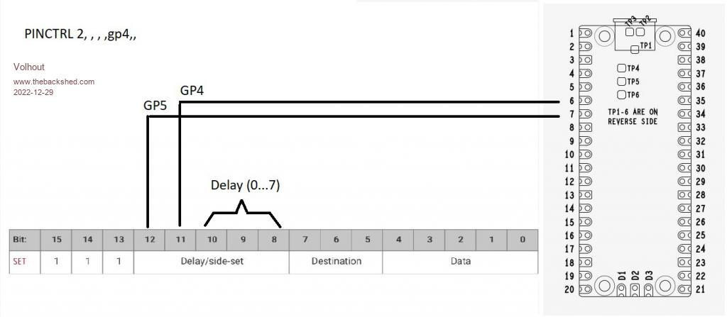 Side set is a blessing, and a burden. Once you decide to use side set, you can write compacter programs, or faster, or more capable, but you have to configure the side set field in EACH instruction in that state machine. Forget one, and side set will set the pin(s) to 0...unexpected... note: there is a mode where 1 bit in the delay/side set field is used a side set enable bit, but we do not use that mode here as you have to sacrifice 1 precious bit in the 5 bit field. Note that SIDE SET range and SET range are independent in the configuration. Ranges can be identical, they can overlap, but they can also be adjacent. So a SET instruction can SET 5 pins, and SIDE SET 5 pins, so it can control 10 pins. SIDE SET pins are set to output the same instruction as SET pins. If we look at the previous GATE PULS example, there where 2 instructions to SET the GATE pin high and low. These instructions can be replaced by the SIDE SET in other instructions. GATE PULSE using SET (chapter 7) 'line code comment ' 0 Ā Ā E081 Ā set GP2 output, note GP2 is assigned in pinctrl '.wrap target ' 1 Ā Ā 80A0 Ā PULL OSR blocking ' 2 Ā Ā A027 Ā MOV OSR->X ' 3 Ā Ā E000 Ā SET GP2 low ' 4 Ā Ā 0044 Ā JMP (X<>0) X-- line 4 ' 5 Ā Ā E001 Ā SET GP2 high '.wrap GATE PULSE using SIDE SET for GP2 Lets first detail out one instruction (most significant bit in delay field is side set bit): PULL OSR blocking, side(1) : 100 10000 1 0 1 00000 = 1001 0000 1010 0000 = &h90A0 'line code comment ' 0 Ā Ā E081 Ā set GP2 output, no side set needed (not in loop) '.wrap target ' 1 Ā Ā 90A0 Ā PULL OSR blocking, side(1) ' 2 Ā Ā B027 Ā MOV OSR->X, side(1) ' 3 Ā Ā 0043 Ā JMP (X<>0) X-- line 4 .side(0) '.wrap This solution has benefit in that it is more compact, and does not suffer from the clock cycle in the SET instructions. The associated configuration would be: EXECCTRL 0,1,3 (wrap target =1, wrap =3) PINCTRL 1,1,,,gp2,gp2, (SET and SIDE SET are identical we use SET to force the pin to output.) Below program shows the gate pulse generator (PIO 1.2) in combination with the actual counter (PIO 1.3). All techniques in previous chapters is used. Please try to understand the PIO 1.3 counter code. It has - count up through inverted count down - WAIT for signal from GATE and input signal - conditional jumps - push ISR - side set The PIO 1.3 code uses SIDE SET in the counter, to communicate via GP3 to MMBasic that it did not find even 1 pulse in the gate time period, as there is no signal. The code: 'Frequency counter using RP2040 PIO 'PIO machine 1.2 generates a progr. gate signal on GP2 (side set pin GP2) 'PIO machine 1.3 uses the gate signal to count GP0 pulses, GP3 is NO SIGNAL 'PIO program and configuration ------------------------------------------------------ 'PIO 1.2 (gate) 'adress Ā Ādata Ā mnemonics Ā Ā Ā Ā Ā Ā Ā Ā Ā Ā Ā Ā comment ' Ā&h10 Ā ĀE084 Ā set pindir 00100 Ā Ā Ā Ā Ā Ā Ā Ā Ā'set GP2 to output, base=GP0 '.wrap target ' Ā&h11 Ā Ā90A0 Ā pull block .side(1) Ā Ā Ā Ā Ā Ā Ā 'pull data from FIFO into OSR when available ' Ā&h12 Ā ĀB027 Ā mov(x,osr) .side(1) Ā Ā Ā Ā Ā Ā Ā 'load gate time (in clock pulses) from osr ' Ā&h13 Ā Ā0053 Ā jmp(x_dec, this line) .side(0) Ā Ā'1 cycle count down + gate low '.wrap 'PIO 1.3 (count) ' Ā&h14 Ā ĀE088 Ā set pindirs 01000 Ā Ā Ā Ā Ā Ā Ā Ā 'GP3 output, base is GP0) '.wrap target ' Ā&h15 Ā ĀA02B Ā mov(x,-1) .side(0) Ā Ā Ā Ā Ā Ā Ā Ā'x = -1 (clear counter) ' Ā&h16 Ā Ā2082 Ā wait(1,gp2) .side(0) Ā Ā Ā Ā Ā Ā Ā'sync to GATE signal ' Ā&h17 Ā Ā2002 Ā wait(0,gp2) .side(0) Ā Ā Ā Ā Ā Ā Ā'detect falling edge of gate signal ' Ā&h18 Ā Ā3000 Ā wait(0,gp0) .side(1) Ā Ā Ā Ā Ā Ā Ā'wait for risig edge input signal ' Ā&h19 Ā Ā3080 Ā wait(1,gp0) .side(1) Ā Ā Ā Ā Ā Ā Ā'wait for falling edge input signal ' Ā&h1A Ā Ā00DC Ā jmp(gp2, to 0x1c) .side(0) Ā Ā Ā Ā'continue counting (gate epuls ended ?) ' Ā&h1B Ā Ā0058 Ā jmp(x_dec, to 0x18) .side(0) Ā Ā Ā'yes, count next pulse input ' Ā&h1C Ā ĀA0C9 Ā mov(isr,-x) .side(0) Ā Ā Ā Ā Ā Ā Ā'copy counter to isr ' Ā&h1D Ā Ā8000 Ā push noblock .side(0) Ā Ā Ā Ā Ā Ā 'get value to FIFO '.wrap 'this is above program in data statements dim a%(7)=(0,0,0,0,&h0053B02790A0E084,&h20022082A02BE088,&h005800DC30803000,&h8000A0C9) 'SETUP code setpin gp0,pio1 Ā Ā Ā Ā Ā'frequency counter input setpin gp2,pio1 Ā Ā Ā Ā Ā'gate signal setpin gp3,pio1 Ā Ā Ā Ā Ā'no signal output used to display input signal missing 'program above code in the chip in PIO 1 pio program 1,a%() 'PIO configuration ------------------------------------------------------------------------- 'PIO 1.2 f2=1e6 Ā Ā Ā Ā Ā Ā Ā Ā Ā Ā Ā Ā Ā Ā Ā Ā'1 MHz frequency gate resolution e2=pio(execctrl 0,&h11,&h13) Ā Ā Ā Ā Ā'wrap target &h11, wrap &h13 p2=Pio(pinctrl 1,1,,,gp2,gp0,) Ā Ā Ā Ā'GP2 side set, GP0 SET (for pindirs) pio init machine 1,2,f2,p2,e2,0,&h10 Ā'start from 0x10 'PIO 1.3 f3=63e6 Ā Ā Ā Ā Ā Ā Ā Ā Ā Ā Ā Ā Ā Ā Ā '63 MHz frequency e3=pio(execctrl 2,&h15,&h1d) Ā Ā Ā Ā Ā'gp2 is PIN for cond jmp. wrap target &h15, wrap &h1D p3=Pio(pinctrl 1,1,,gp0,gp3,gp0,) Ā Ā 'GP0 base for inputs, GP0 out for SET/SIDE pio init machine 1,3,f3,p3,e3,0,&h14 Ā'start from 0x14 'Start both PIO sequencers PIO start 1,2 'this will wait for data to arrive in FIFO, then generate 1 gate PIO start 1,3 'this will start counter, waiting on adress &h17 for GP2 gate to become low 'MMBASIC MAIN CODE -------------------------------------------------------------------------- 'generate a test frequency on GP3, for testing of the counter setpin gp4,pwm pwm 2,15000000,50 Ā Ā Ā Ā Ā Ā Ā Ā 'change 15000000 to test different frequencies. Ā Ā Ā Ā Ā Ā Ā Ā Ā Ā Ā Ā Ā Ā Ā Ā Ā '15MHz PLL generates 15.75MHz dues to divider settings inside the PLL 'variables and constants used in the counter dim r%(3),c% Ā Ā Ā Ā Ā Ā Ā Ā Ā Ā Ā Ā'define variables, r%() only used to empty fifo gate_time = 0.1 Ā Ā Ā Ā Ā Ā Ā Ā Ā Ā 'seconds gate_clocks% = gate_time*f2 - 1 Ā Ā 'for 1MHz PIO clock as integer (n counts (n-1...0)) 'this loop does the actual counting do Ā'first check if there is no input signal. PIO 1.3 will be stuck at instruction &h18 or &h19 and Ā'side set pin GP3 will be high. Āif pin(gp3)=1 then Ā Ā Āprint "no input signal" Ā Āpause 200 Ā Āelse Ā Ā Ā'put gate time in PIO 1.2 OSR (gate_ime is specified in PIO cycles: gate_clocks%) Ā Āpio read 1,3,4,r%() Ā Ā Ā Ā Ā Ā Ā 'empty fifo from rubbish (only needed at start) Ā Āpio write 1,2,1,gate_clocks% Ā Ā Ā'this starts the gate pulse generator, single pulse Ā Ā'wait gate time + few ms for printing data Ā Āpause (1000*gate_time + 200) Ā Ā'get FIFO value Ā Āpio read 1,3,1,c% Ā Ā Ā Ā Ā Ā Ā Ā 'read value from FIFO (there is only 1 value in it) Ā Āc%=c%/gate_time Ā Ā Ā Ā Ā Ā Ā Ā Ā 'convert or Hz Ā Ā'print frequency value Ā Āprint "GP1 frequency = ";c%;" Hz" Āend if loop The exercise for next week is to combine this with the pulse and period measurement code into one big multi function counter. Next Chapter : serial input (SPI) using ISR, Edited 2022-12-29 06:54 by Volhout PicomiteVGA PETSCII ROBOTS |
||||
| phil99 Guru Joined: 11/02/2018 Location: AustraliaPosts: 3288 |
Puzzled. ? mm.info(cpuspeed) 126000000 > RUN GP1 frequency = Ā40036816480 Hz GP1 frequency = Ā40036816480 Hz GP1 frequency = Ā40036816480 Hz GP Did not expect 40GHz! Edit Dodgy breadboard. Now with 0 ohms between GP1 & GP4. > RUN GP1 frequency = Ā70 Hz GP1 frequency = Ā70 Hz GP1 frequency = Ā70 Hz Edited 2022-12-29 17:26 by phil99 |
||||
| Volhout Guru Joined: 05/03/2018 Location: NetherlandsPosts: 5922 |
Hi phil99, I apologize., there was an error in the program, and I did correct some text (input was GP0 not GP1). The error was that I wanted to set the GP2 pin direction in a SET statement that had as base GP0, was 1 pin wide. And it worked (kind of) on my breadboard , but I did not re-power the breadboard to make absolutely sure it worked also for others. GP4 provides the test signal GP0 = input GP2 = gate GP3 = pulses counted (should alternate with GATE) and high when nothing on GP0 I run the pico CPU at 126MHz 'Frequency counter using RP2040 PIO Ā 'PIO machine 1.2 generates a progr. gate signal on GP2 (side set pin GP2) 'PIO machine 1.3 uses the gate signal to count GP0 pulses, GP3 is NO SIGNAL Ā 'PIO program and configuration ------------------------------------------------------ Ā 'PIO 1.2 (gate) 'adress Ā Ādata Ā mnemonics Ā Ā Ā Ā Ā Ā Ā Ā Ā Ā Ā Ā comment ' Ā&h10 Ā ĀE081 Ā set pindir 00001 Ā Ā Ā Ā Ā Ā Ā Ā Ā'set GP2 to output '.wrap target ' Ā&h11 Ā Ā90A0 Ā pull block .side(1) Ā Ā Ā Ā Ā Ā Ā 'pull data from FIFO into OSR when available ' Ā&h12 Ā ĀB027 Ā mov(x,osr) .side(1) Ā Ā Ā Ā Ā Ā Ā 'load gate time (in clock pulses) from osr ' Ā&h13 Ā Ā0053 Ā jmp(x_dec, this line) .side(0) Ā Ā'1 cycle count down + gate low '.wrap Ā Ā 'PIO 1.3 (count) ' Ā&h14 Ā ĀE081 Ā set pindirs 00001 Ā Ā Ā Ā Ā Ā Ā Ā 'GP3 output '.wrap target ' Ā&h15 Ā ĀA02B Ā mov(x,-1) .side(0) Ā Ā Ā Ā Ā Ā Ā Ā'x = -1 (clear counter) ' Ā&h16 Ā Ā2082 Ā wait(1,gp2) .side(0) Ā Ā Ā Ā Ā Ā Ā'sync to GATE signal ' Ā&h17 Ā Ā2002 Ā wait(0,gp2) .side(0) Ā Ā Ā Ā Ā Ā Ā'detect falling edge of gate signal ' Ā&h18 Ā Ā3000 Ā wait(0,gp0) .side(1) Ā Ā Ā Ā Ā Ā Ā'wait for risig edge input signal ' Ā&h19 Ā Ā3080 Ā wait(1,gp0) .side(1) Ā Ā Ā Ā Ā Ā Ā'wait for falling edge input signal ' Ā&h1A Ā Ā00DC Ā jmp(gp2, to 0x1c) .side(0) Ā Ā Ā Ā'continue counting (gate epuls ended ?) ' Ā&h1B Ā Ā0058 Ā jmp(x_dec, to 0x18) .side(0) Ā Ā Ā'yes, count next pulse input ' Ā&h1C Ā ĀA0C9 Ā mov(isr,-x) .side(0) Ā Ā Ā Ā Ā Ā Ā'copy counter to isr ' Ā&h1D Ā Ā8000 Ā push noblock .side(0) Ā Ā Ā Ā Ā Ā 'get value to FIFO '.wrap Ā 'this is above program in data statements Ādim a%(7)=(0,0,0,0,&h0053B02790A0E081,&h20022082A02BE081,&h005800DC30803000,&h8000A0C9) Ā Ā 'SETUP code Āsetpin gp0,pio1 Ā Ā Ā Ā Ā'frequency counter input Āsetpin gp2,pio1 Ā Ā Ā Ā Ā'gate signal Āsetpin gp3,pio1 Ā Ā Ā Ā Ā'no signal output used to display input signal missing Ā 'program above code in the chip in PIO 1 Āpio program 1,a%() Ā Ā 'PIO configuration ------------------------------------------------------------------------- Ā 'PIO 1.2 Āf2=1e6 Ā Ā Ā Ā Ā Ā Ā Ā Ā Ā Ā Ā Ā Ā Ā Ā'1 MHz frequency gate resolution Āe2=pio(execctrl 0,&h11,&h13) Ā Ā Ā Ā Ā'wrap target &h11, wrap &h13 Āp2=Pio(pinctrl 1,1,,,gp2,gp2,) Ā Ā Ā Ā'GP2 side set, GP0 SET (for pindirs) Āpio init machine 1,2,f2,p2,e2,0,&h10 Ā'start from 0x10 Ā 'PIO 1.3 Āf3=63e6 Ā Ā Ā Ā Ā Ā Ā Ā Ā Ā Ā Ā Ā Ā Ā '63 MHz frequency Āe3=pio(execctrl 2,&h15,&h1d) Ā Ā Ā Ā Ā'gp2 is PIN for cond jmp. wrap target &h15, wrap &h1D Āp3=Pio(pinctrl 1,1,,gp0,gp3,gp3,) Ā Ā 'GP0 base for inputs, GP0 out for SET/SIDE Āpio init machine 1,3,f3,p3,e3,0,&h14 Ā'start from 0x14 Ā Ā 'Start both PIO sequencers ĀPIO start 1,2 'this will wait for data to arrive in FIFO, then generate 1 gate ĀPIO start 1,3 'this will start counter, waiting on adress &h17 for GP2 gate to become low Ā Ā Ā 'MMBASIC MAIN CODE -------------------------------------------------------------------------- Ā 'generate a test frequency on GP4, for testing of the counter Āsetpin gp4,pwm Āpwm 2,15000000,50 Ā Ā Ā Ā Ā Ā Ā Ā 'change 15000000 to test different frequencies. '15MHz PLL generates 15.75MHz dues to divider settings inside the PLL Ā Ā Ā Ā Ā 'variables and constants used in the counter Ādim r%(3),c% Ā Ā Ā Ā Ā Ā Ā Ā Ā Ā Ā Ā'define variables, r%() only used to empty fifo Āgate_time = 0.1 Ā Ā Ā Ā Ā Ā Ā Ā Ā Ā 'seconds Āgate_clocks% = gate_time*f2 - 1 Ā Ā 'for 1MHz PIO clock as integer (n counts (n-1...0)) Ā Ā 'this loop does the actual counting Ādo Ā Ā Ā Ā'first check if there is no input signal. PIO 1.3 will be stuck at instruction &h18 or &h19 and Ā Ā'side set pin GP3 will be high. Ā Āif pin(gp3)=1 then Ā Ā Ā Ā Āprint "no input signal" Ā Ā Āpause 200 Ā Ā Ā Āelse Ā Ā 'put gate time in PIO 1.2 OSR (gate_ime is specified in PIO cycles: gate_clocks%) Ā Āpio read 1,3,4,r%() Ā Ā Ā Ā Ā Ā Ā 'empty fifo from rubbish (only needed at start) Ā Āpio write 1,2,1,gate_clocks% Ā Ā Ā'this starts the gate pulse generator, single pulse Ā Ā 'wait gate time + few ms for printing data Ā Āpause (1000*gate_time + 200) Ā Ā 'get FIFO value Ā Āpio read 1,3,1,c% Ā Ā Ā Ā Ā Ā Ā Ā 'read value from FIFO (there is only 1 value in it) Ā Āc%=c%/gate_time Ā Ā Ā Ā Ā Ā Ā Ā Ā 'convert or Hz Ā Ā 'print frequency value Ā Āprint "GP0 frequency = ";c%;" Hz" Ā Āend if Ā Ā Āloop Edited 2022-12-29 17:50 by Volhout PicomiteVGA PETSCII ROBOTS |
||||
| phil99 Guru Joined: 11/02/2018 Location: AustraliaPosts: 3288 |
Thanks for the updated version. Perfect. Edit " pwm 2,15000000,50 'change 15000000 to test different frequencies. '15MHz PLL generates 15.75MHz dues to divider settings inside the PLL" Yes, replacing PWM freq. with 63e6 / 4 gives the same output as 15e6. Saved 4456 bytes GP0 frequency = 15749990 Hz Edited 2022-12-30 09:52 by phil99 |
||||
| phil99 Guru Joined: 11/02/2018 Location: AustraliaPosts: 3288 |
Mashing it all together. 'PIO 0,1,2,3 'PIO measure pulse from GP0 'The program uses a PMW at GP0 output to generate a test frequency, just to test the function ' The PIO program ------------------------------------------------------------------- 'configure the PIO sequencer clock and pin registers p0=0 Ā Ā Ā Ā Ā Ā Ā Ā Ā'no IO pins used except PIN in JMP (not part of this register) e0=Pio(execctrl 0,0,5) Ā Ā Ā'use pin gp0, wrap target = 0, wrap = 6 f0=63e6 Ā Ā Ā Ā Ā Ā Ā Ā Ā Ā Ā '63MHz PIO frequency for high resolution ' PIO1 program, measure period on GP0 (depends on PIN setting EXECCTRL register) ' the period is 2*TC*count%, where TC= PIO clock frequency ' 'line Ā code Ā Ācomment '.wrap ' 0 Ā Ā A02B Ā ĀMov X=-NULL ' 1 Ā Ā 2080 Ā ĀWait until GP0=1 ' 2 Ā Ā 0043 Ā ĀJMP (x<>0) x--, 3 (always go to next instruction, decrement x) ' 3 Ā Ā 00C2 Ā ĀJMP (GP0=1), 2 ' 4 Ā Ā A0C9 Ā ĀMOV ISR = -X (invert result) ' 5 Ā Ā 8000 Ā ĀPush noblock (ISR->FIFO) '.wrap target PIO program line 1,0,&b1010000000101011 '&hA02B PIO program line 1,1,&b0010000010000000 '&h2080 PIO program line 1,2,&b0000000001000011 '&h0043 PIO program line 1,3,&b0000000011000010 '&h00C2 PIO program line 1,4,&b1010000011001001 '&hA0C9 PIO program line 1,5,&b1000000000000000 '&h8000 'PIO1 and setup the machine, and start it. PIO init machine 1,0,f0,p0,e0,,0 'PIO measure pause (pulse low) from GP0 'The program uses a PMW at GP0 output to generate a test frequency, just to test the function ' The PIO program ------------------------------------------------------------------- ' configure the PIO 1 sequencer 1 clock and pin registers p1=0 Ā Ā Ā Ā Ā Ā Ā Ā Ā'no IO pins used except PIN in JMP (not part of this register) e1=Pio(execctrl 0,6,11) Ā Ā Ā'use pin gp0, wrap target = 6, wrap = 11 f1=63e6 Ā Ā Ā Ā Ā Ā Ā Ā Ā Ā Ā '63MHz PIO frequency for high resolution ' PIO1 program, measure pause on GP0 (depends on PIN setting EXECCTRL register) ' The pause is 2*TC*count%, where TC = PIO clock frequency ' The state machine code starts at address 6 since adress 0..5 are occupied by the PULSE ' measurement designed previously, running on state machine 0. ' ' 'line Ā code Ā Ācomment '.wrap target ' 6 Ā Ā A02B Ā ĀMov X=-NULL ' 7 Ā Ā 2000 Ā ĀWait until GP0=0 ' 8 Ā Ā 00CA Ā ĀJMP (GP0=1) 10 Ā Ā (jump out of the loop when GP0=1) ' 9 Ā Ā 0048 Ā ĀJMP (X<>0) X--, 2 Ā(decrement X and always jump back to 8) ' A Ā Ā A0C9 Ā ĀMOV ISR = -X Ā Ā Ā (invert result) ' B Ā Ā 8000 Ā ĀPush noblock Ā Ā Ā (ISR->FIFO) '.wrap target PIO program line 1,6,&hA02B' &b1010000000101011 PIO program line 1,7,&h2000' &b0010000000000000 PIO program line 1,8,&h00CA' &b0000000011001010 PIO program line 1,9,&h0048' &b0000000001001000 PIO program line 1,10,&hA0C9' &b1010000011001001 PIO program line 1,11,&h8000' &b1000000000000000 'PIO1 and setup the machine, and start it from address 6. PIO init machine 1,1,f1,p1,e1,,6 'Frequency counter using RP2040 PIO 'PIO machine 1.2 generates a progr. gate signal on GP2 (side set pin GP2) 'PIO machine 1.3 uses the gate signal to count GP0 pulses, GP3 is NO SIGNAL 'PIO program and configuration ------------------------------------------------------ 'PIO 1.2 (gate) 'adress Ā Ādata Ā mnemonics Ā Ā Ā Ā Ā Ā Ā Ā Ā Ā Ā Ā comment PIO program line 1,&h10,&hE081' Ā set pindir 00001 Ā Ā Ā Ā Ā Ā Ā Ā Ā'111 00000 100 00001 set GP2 to output '.wrap target PIO program line 1,&h11,&h90A0' Ā pull block .side(1) Ā Ā Ā Ā Ā Ā Ā '100 10000 101 00000 pull data from FIFO into OSR when available PIO program line 1,&h12,&hB027' Ā mov(x,osr) .side(1) Ā Ā Ā Ā Ā Ā Ā '101 10000 001 00111 load gate time (in clock pulses) from osr PIO program line 1,&h13,&h0053' Ā jmp(x_dec, this line) .side(0) Ā Ā'000 00000 101 00111 cycle count down + gate low '.wrap 'PIO 1.3 (count) PIO program line 1,&h14,&hE081' Ā set pindirs 00001 Ā Ā Ā Ā Ā Ā Ā Ā '111 00000 100 00001 GP3 output '.wrap target PIO program line 1,&h15,&hA02B' Ā mov(x,-1) .side(0) Ā Ā Ā Ā Ā Ā Ā Ā'101 00000 001 01011 x = -1 (clear counter) PIO program line 1,&h16,&h2082' Ā wait(1,gp2) .side(0) Ā Ā Ā Ā Ā Ā Ā'001 00000 100 00010 sync to GATE signal PIO program line 1,&h17,&h2002' Ā wait(0,gp2) .side(0) Ā Ā Ā Ā Ā Ā Ā'001 00000 000 00010 detect falling edge of gate signal PIO program line 1,&h18,&h3000' Ā wait(0,gp0) .side(1) Ā Ā Ā Ā Ā Ā Ā'001 10000 000 00000 wait for risig edge input signal PIO program line 1,&h19,&h3080' Ā wait(1,gp0) .side(1) Ā Ā Ā Ā Ā Ā Ā'001 10000 100 00000 wait for falling edge input signal PIO program line 1,&h1A,&h00DC' Ā jmp(gp2, to 0x1c) .side(0) Ā Ā Ā Ā'000 00000 110 11100 continue counting (gate epuls ended ?) PIO program line 1,&h1B,&h0058' Ā jmp(x_dec, to 0x18) .side(0) Ā Ā Ā'000 00000 010 11000 yes, count next pulse input PIO program line 1,&h1C,&hA0C9' Ā mov(isr,-x) .side(0) Ā Ā Ā Ā Ā Ā Ā'101 00000 110 01001 copy counter to isr PIO program line 1,&h1D,&h8000' Ā push noblock .side(0) Ā Ā Ā Ā Ā Ā '100 00000 000 00000 get value to FIFO '.wrap 'this is above program in data statements ' dim a%(7)=(0,0,0,0,&h0053B02790A0E081,&h20022082A02BE081,&h005800DC30803000,&h8000A0C9) 'SETUP code setpin gp0,pio1 Ā Ā Ā Ā Ā'frequency counter input setpin gp2,pio1 Ā Ā Ā Ā Ā'gate signal setpin gp3,pio1 Ā Ā Ā Ā Ā'no signal output used to display input signal missing 'program above code in the chip in PIO 1 ' pio program 1,a%() 'PIO configuration ------------------------------------------------------------------------- 'PIO 1.2 f2=1e6 Ā Ā Ā Ā Ā Ā Ā Ā Ā Ā Ā Ā Ā Ā Ā Ā'1 MHz frequency gate resolution e2=pio(execctrl 0,&h11,&h13) Ā Ā Ā Ā Ā'wrap target &h11, wrap &h13 p2=Pio(pinctrl 1,1,,,gp2,gp2,) Ā Ā Ā Ā'GP2 side set, GP0 SET (for pindirs) pio init machine 1,2,f2,p2,e2,0,&h10 Ā'start from 0x10 'PIO 1.3 f3=63e6 Ā Ā Ā Ā Ā Ā Ā Ā Ā Ā Ā Ā Ā Ā Ā '63 MHz frequency e3=pio(execctrl 2,&h15,&h1d) Ā Ā Ā Ā Ā'gp2 is PIN for cond jmp. wrap target &h15, wrap &h1D p3=Pio(pinctrl 1,1,,gp0,gp3,gp3,) Ā Ā 'GP0 base for inputs, GP0 out for SET/SIDE pio init machine 1,3,f3,p3,e3,0,&h14 Ā'start from 0x14 'Start both PIO sequencers PIO start 1,0 PIO start 1,1 PIO start 1,2 'this will wait for data to arrive in FIFO, then generate 1 gate PIO start 1,3 'this will start counter, waiting on adress &h17 for GP2 gate to become low 'The MMBasic program -------------------------------------------------------- 'generate a test frequency on GP4, for testing of the counter setpin gp4,pwm pwm 2,15000,50 Ā Ā Ā Ā Ā Ā Ā Ā 'change 15000 to test different frequencies. '15kHz PLL generates 15.?kHz dues to divider settings inside the PLL 'variables and constants used in the counter dim r%(3),c% Ā Ā Ā Ā Ā Ā Ā Ā Ā Ā Ā Ā'define variables, r%() only used to empty fifo gate_time = 0.1 Ā Ā Ā Ā Ā Ā Ā Ā Ā Ā 'seconds gate_clocks% = gate_time*f2 - 1 Ā Ā 'for 1MHz PIO clock as integer (n counts (n-1...0)) 'The actual measurement routine DIM count% 'read the top of the PIO FIFO one word at at time. Since you start measuring at a 'random moment, the first reading can be wrong (incomplete cycle). Do ĀPIO READ 1,0,1,count% Ā Ā 'reads the fifo register Āpulsewidth = 2 * (1e6/f0) * count% ĀPIO READ 1,1,1,count% Ā Ā 'reads the fifo register Āpausewidth = 2 * (1e6/f1) * count% ĀPeriod = pulsewidth+pausewidth Āprint "Mark ";pulsewidth;" us", "Space ";pausewidth;" us","Period ";Period;" us","F "1e6 / Period;" Hz" ĀPause 200 Ā Ā 'first check if there is no input signal. PIO 1.3 will be stuck at instruction &h18 or &h19 and Ā 'side set pin GP3 will be high. Ā if pin(gp3)=1 then Ā Ā Ā print "no input signal" Ā Ā pause 200 Ā Ā else Ā 'put gate time in PIO 1.2 OSR (gate_ime is specified in PIO cycles: gate_clocks%) Ā pio read 1,3,4,r%() Ā Ā Ā Ā Ā Ā Ā 'empty fifo from rubbish (only needed at start) Ā pio write 1,2,1,gate_clocks% Ā Ā Ā'this starts the gate pulse generator, single pulse Ā 'wait gate time + few ms for printing data Ā pause (1000*gate_time + 200) Ā 'get FIFO value Ā pio read 1,3,1,c% Ā Ā Ā Ā Ā Ā Ā Ā 'read value from FIFO (there is only 1 value in it) Ā c%=c%/gate_time Ā Ā Ā Ā Ā Ā Ā Ā Ā 'convert or Hz Ā 'print frequency value Ā print "GP0 frequency = ";c%;" Hz" Ā end if Loop While Inkey$="" PIO stop 1,0 PIO stop 1,1 PIO stop 1,2 PIO stop 1,3 End Edited 2022-12-31 15:56 by phil99 |
||||
| Volhout Guru Joined: 05/03/2018 Location: NetherlandsPosts: 5922 |
We have all ingredients to make it a counter. Now we need the GUI, for an LCD. And for phill99, and all that tried exercises: This is the maek/space/frequency counter. For the frequency ratio counter (using GP1 as B input) a possible solution is to adapt the counter(not the gate pulse, you need only 1) as a separate counter(using its own statemachine) and dividing in MMBasic A by B. This will require reprogramming the PIO since we used all statemachines. So frequency ratio selection reprograms PIO. There are 2 ways: 1 copy the pio 1.3 code and adapt for pio 1.0 ang gp1 2 change the program in pio1.3 so it becomes universal. A way to do that is chang the 2 WAIT for gate pulse, into JMPs that sense the pin asigned in EXECCTRL... Reason for option 2 is: current 1.3 program uses gp0 and gp2 as inputs. The new code must use gp1 and gp2 as inputs. That is different program code when using WAIT. But if you use JMP you can leave the program the same, and only change configuration. Edited 2022-12-31 19:11 by Volhout PicomiteVGA PETSCII ROBOTS |
||||
| Bleep Guru Joined: 09/01/2022 Location: United KingdomPosts: 800 |
Thanks Volhout, I've been following your course with much interest and have now, at last, succeeded in getting my NioPixel (WS2812) driver working. The attached code written in MMBasic will drive a string of ~340 (or more) NioPixels instantaneously all Red, then all Green, then all Blue, with a 200mS delay between each colour change, now the challenge to make it more interesting. :-) Regards, Kevin. video 'PIO WS2812 driver on GP0 ' ' The PIO program ------------------------------------------------------------------- 'Set GPIO to GP0 SetPin gp0,pio1 'configure the PIO sequencer clock and pin registers e0=Pio(execctrl 0,1,4) p0=Pio(pinctrl 1,1,,,gp0,gp0,) Ā Ā'GP0 side set, GP0 SET (for pindirs) f0=Pio(shiftctrl 0,0,0,1) Ā Ā Ā Ā 'Set Auto Pull at 32bits (0) fr0=5000000 Ā Ā Ā Ā Ā Ā Ā Ā Ā Ā Ā '5MHz PIO frequency, lowest I could go with my pixels 'This code relies on AutoPull when all 32 bits have been read from X 'line Ā Bin Ā Ā Ā Ā Ā Ā code Ā Ā Ā Ā Ā Ā Ā Ā Ā Ā Ā Ā Ā Ā Ācomment '0 Ā1110 0000 1000 0001 'set GP0 output, side(0), Ā Ā Ā Ā 'note GP0 is assigned in pinctrl '.wrap_target '1 Ā0110 0002 0010 0001 'out x, 1bit, side(0), dly 2 or 1 'put one bit in x side set 0 '2 Ā0001 0001 0010 0011 'jmp !x to 4, side(1), dly 1 or 1 'jump if not X (ie 0) side set 1 '3 Ā0001 0004 0000 0000 'jmp to 1, side(1), dly 1 or 2 Ā Ā'jump to 1 side set 1 '4 Ā1010 0004 0100 0010 'MOV Y to Y side(0), dly 2 or 2 Ā 'Nop delay side set 0 'wrap PIO program line 1,0,&hEF81 PIO program line 1,1,&h6121 PIO program line 1,2,&h1124 PIO program line 1,3,&h1101 PIO program line 1,4,&hA142 'PIO1.0 Āsetup the machine. PIO init machine 1,0,fr0,p0,e0,f0,0 'LED data GRBG RBGR BGRB GRBG Dim Integer ct(3)=(&h00000100,&h00010000,&h01000001,&h00000100) 'The MMBasic program -------------------------------------------------------- Do PIO start 1,0 Ā'start the PIO For b=0 To 86 ĀPIO WRITE 1,0,3,ct(0),ct(1),ct(2) 'writes led colours to fifo Next PIO Write 1,0,1,&h00000000 Ā' Haven't worked out why I need this to flush? ct(3)=ct(0):ct(0)=ct(1):ct(1)=ct(2):ct(2)=ct(3) ' rotate the colours PIO stop 1,0 Ā 'stop the pio Pause 200 Loop While Inkey$="" End Edited 2023-01-01 04:29 by Bleep |
||||
| Volhout Guru Joined: 05/03/2018 Location: NetherlandsPosts: 5922 |
Wauw Bleep! That is good work. You did not use the shift OUT, but made your own shift. Good thinking, and compact code. You could add a little explanation of the timing requirements (bit times) so it is clear to all why the code is as it is.... Again, compliments... Volhout PicomiteVGA PETSCII ROBOTS |
||||
| karlelch Guru Joined: 30/10/2014 Location: GermanyPosts: 328 |
I discovered this thread only recently. Great read! Excellent tutorial! Thanks @Volhout! |
||||
| Bleep Guru Joined: 09/01/2022 Location: United KingdomPosts: 800 |
Hi Volhout, I can't make any claims on the PIO code, that's straight out of the Pico SDK I was stuck on how to set up the PIO to do side set, which you've explained and how to auto pull from fifo, in Basic. I've just realised I left my comments on the instruction delays in, which are now wrong, as I ended up with just 1 extra delay count for all instructions in the main loop, that gave me the best timings for my NeoPixels at a PIO clock of 5MHz. I tried to run the PIO as slow as I could so that the Basic could keep up with feeding it data! As for NeoPixels they are quite fussy as to their timings, there is quite a lot of difference between different manufacturers. It seems to boil down to approximately this. Timings to produce a 0 bit Ā Ā Ā Ā Ā Ā Ā Ā Āmin Ā Ā typ Ā Ā max T0H Ā Ā 0 code ,high voltage time Ā Ā Ā 200 Ā Ā 350 Ā Ā 500 Āns T0L Ā ĀĀ 0 code ,low voltage time Ā Ā Ā Ā650 Ā Ā 800 Ā Ā 950 Āns Timings to produce a 1 bit T1H Ā Ā 1 code ,high voltage time Ā Ā Ā 550 Ā Ā 700 Ā Ā 850 Āns T1L Ā ĀĀ 1 code ,low voltage time Ā Ā Ā Ā450 Ā Ā 600 Ā Ā 750 Āns Timing for a reset. RES Ā Ā Ālow voltage time Ā Ā Ā Ā Ā Ā ĀĀ Ā Ā50,000 ns So to produce a 1 bit the data stream needs to be high for 350nS & low for 800nS. To produce a 0 bit the data stream needs to be high for 700nS & low for 600nS. Or there abouts. :-) Reset starts again at the first LED. Regards Kevin. Edited 2023-01-01 09:11 by Bleep |
||||
| Volhout Guru Joined: 05/03/2018 Location: NetherlandsPosts: 5922 |
Dear TBS'ers, For the last 2 chapters in the PIO training course (shifting data IN and shifting data OUT using the FIFO) I have ordered some hardware. In case you want to duplicate the exercises for these chapters, you may want to do the same, or look in your toolbox what you have available. For shifting serial data IN, I will focus on the 4021 shift register (as used in the NES controllers). For shifting data OUT I will use a 74HC(T)595 as demo device. While waiting for the parts to arrive, I will continue to complete the PIO frequency counter project. I have made some changes to it already, while learning on the job. One change I made is in the PULSE and PAUSE (Mark and Space) measurement. Since low frequencies (like 50Hz) have low resolution in frequency measurement, but high resolution in pulse/pause measurement, it is beneficial to use pulse+pause=period to calculate the frequency more accurate. So you need period information and frequency information available at all times to choose the best for high resolution. And since we have only 4 state machines, things have to be re-arranged to meet all functionality. Previous PIO1.0 pulse PIO1.1 pause PIO1.2 gate pulse generator PIO1.3 frequency New PIO1.0 period A (GP0) PIO1.1 pulse A (GP0) -or- frequency channel B (running PIO1.3 program with config for GP1) PIO1.2 gate pulse generator PIO1.3 frequency channel A (GP0) So PIO 1.0, 1.2, 1.3 are always running, PIO 1.1 only wen needed, and it can change it's function by selecting a different configuration. The code below shows the current status (experiment when you feel like it). The PIO1.1 selection now is done by commenting out lines. this will change once I start working on the GUI (se todo list). Again: this is WORK IN PROGRESS 'Multi function counter using RP2040 PIO Ā 'Version control ------------------------------------------------------------------- 'Version Ā ĀFeatures ' Ā6 Ā Ā Ā Single frequency measurement, posted on TBS in PIO training course ' 10 Ā Ā Ā Dual frequency counter using PIO 1.1, 1.2, 1.3 and ratio calculation ' 11 Ā Ā Ā Added Period measurement and Pulse measurement 'todo ------------------------------------------------------------------------------ ' make function selector (PIO 1.1 config) ' calculate resolution and adapt print statement to show only relevant info (MMBasic) ' auto switch period/frequency basis depending resolution (MMBasic) ' make LCD GUI (develop on VGA picomite ?) ' develop hardware (input circuits using 74LVC132 or 74LVC14 and amplifier for AC-A) ' START/STOP on A/B function (MMBasic ? / PIO ?) ' Run pico at higher clock and adapt f0...f3 for more bandwidth/resolution Ā Ā 'PIO usage ------------------------------------------------------------------------- ' 'PIO machine 1.0 measures period GP0 signal ' 'PIO machine 1.1 has 2 configurations ' Ā uses the GP2 gate signal to count GP1 pulses, GP4 is NO GP1 SIGNAL ' Ā -or- ' Ā measures PULSE width for time measurements (PAUSE = PERIOD-PULSE) ' 'PIO machine 1.2 generates a progr. gate signal on GP2 (side set pin GP2) ' Ā ĀPIO machine 1.2 sets GP2,GP3,GP4 output for all state machines 1.1, 1.2 and 1.3 ' 'PIO machine 1.3 uses the GP2 gate signal to count GP0 pulses, GP3 is NO GP0 SIGNAL ' 'PIO 1.0, 1.2 and 1.3 always run, depending the measurement selection PIO 1.1 changes 'function. Ā Ā Ā 'PIO program and configuration ------------------------------------------------------ ' 'PIO 1.0 (period) 'adress Ā Ādata Ā mnemonics Ā Ā Ā Ā Ā Ā Ā Ā Ā Ā Ā Ā comment '.wrap target ' &h00 Ā Ā A02B Ā ĀMov X=-NULL Ā Ā Ā Ā Ā Ā Ā Ā Ā Ā Ā'clear X ' &h01 Ā Ā 0042 Ā ĀJMP (x<>0) x--, 2 Ā Ā Ā Ā Ā Ā Ā Ā'always go to next instruction, decrement x ' &h02 Ā Ā 00C1 Ā ĀJMP (GP0=1), 1 Ā Ā Ā Ā Ā Ā Ā Ā Ā 'high count loop ' &h03 Ā Ā 00C5 Ā ĀJMP (GP0=1) 5 Ā Ā Ā Ā Ā Ā Ā Ā Ā Ā'jump out of the low count loop when GP0=1 ' &h04 Ā Ā 0043 Ā ĀJMP (X<>0) X--, 3 Ā Ā Ā Ā Ā Ā Ā Ā'decrement X and always jump back to 3 ' &h05 Ā Ā A0C9 Ā ĀMOV ISR = -X Ā Ā Ā Ā Ā Ā Ā Ā Ā Ā 'X invert result -> ISR ' &h06 Ā Ā 8000 Ā ĀPush noblock Ā Ā Ā Ā Ā Ā Ā Ā Ā Ā 'ISR->FIFO '.wrap Ā 'PIO 1.1 (pulse) runs this code -or- the code under PIO 1.3 depending the configuration 'adress Ā Ādata Ā mnemonics Ā Ā Ā Ā Ā Ā Ā Ā Ā Ā Ā Ā comment '.wrap target ' &h07 Ā Ā A02B Ā ĀMov X=-NULL Ā Ā Ā Ā Ā Ā Ā Ā Ā Ā Ā'clear X ' &h08 Ā Ā 2080 Ā ĀWait until GP0=1 Ā Ā Ā Ā Ā Ā Ā Ā 'wait for pulse rising edge to start counting ' &h09 Ā Ā 004A Ā ĀJMP (x<>0) x--, &h0A Ā Ā Ā Ā Ā Ā 'always go to next instruction, decrement x ' &h0A Ā Ā 00C9 Ā ĀJMP (GP0=1), 2&h09 Ā Ā Ā Ā Ā Ā Ā 'high count loop ' &h0B Ā Ā A0C9 Ā ĀMOV ISR = -X Ā Ā Ā Ā Ā Ā Ā Ā Ā Ā 'X invert result -> ISR ' &h0C Ā Ā 8000 Ā ĀPush noblock Ā Ā Ā Ā Ā Ā Ā Ā Ā Ā 'ISR->FIFO '.wrap 'not used &h0D...&h13 (7 words) Ā 'PIO 1.2 (gate) 'adress Ā Ādata Ā mnemonics Ā Ā Ā Ā Ā Ā Ā Ā Ā Ā Ā Ā comment ' Ā&h14 Ā ĀE087 Ā set pindir 00111 Ā Ā Ā Ā Ā Ā Ā Ā Ā'set GP2,GP3,GP4 to output for both state machines '.wrap target ' Ā&h15 Ā Ā90A0 Ā pull block .side(1) Ā Ā Ā Ā Ā Ā Ā 'pull data from FIFO into OSR when available ' Ā&h16 Ā ĀB027 Ā mov(x,osr) .side(1) Ā Ā Ā Ā Ā Ā Ā 'load gate time (in clock pulses) from osr ' Ā&h17 Ā Ā0057 Ā jmp(x_dec, this line) .side(0) Ā Ā'1 cycle count down + gate low '.wrap ' 'PIO 1.3 (count) and also PIO 1.1 when ratio is chosen 'adress Ā Ādata Ā mnemonics Ā Ā Ā Ā Ā Ā Ā Ā Ā Ā Ā Ā comment '.wrap target ' Ā&h18 Ā ĀA02B Ā mov(x,-1) .side(0) Ā Ā Ā Ā Ā Ā Ā Ā'x = -1 (clear counter) ' Ā&h19 Ā Ā00D9 Ā jmp(gp2, to 0x19) .side(0) Ā Ā Ā Ā'wait for gate pulse to become low ' Ā&h1A Ā Ā3020 Ā wait(0,gpx) .side(1) Ā Ā Ā Ā Ā Ā Ā'wait rising edge input, index+base IN ' Ā&h1B Ā Ā30A0 Ā wait(1,gpx) .side(1) Ā Ā Ā Ā Ā Ā Ā'wait falling edge input, index+base IN ' Ā&h1C Ā Ā00DE Ā jmp(gp2, to 0x1E) .side(0) Ā Ā Ā Ā'continue counting (gate pulse ended ?) ' Ā&h1D Ā Ā005A Ā jmp(x_dec, to 0x1A) .side(0) Ā Ā Ā'yes, count next pulse input ' Ā&h1E Ā ĀA0C9 Ā mov(isr,-x) .side(0) Ā Ā Ā Ā Ā Ā Ā'copy counter X inverted to ISR ' Ā&h1F Ā Ā8000 Ā push noblock .side(0) Ā Ā Ā Ā Ā Ā 'get value to FIFO '.wrap Ā 'this is above program in data statements Ādim a%(7)=(&h00C500C10042A02B,&hA02B8000A0C90043,&hA0C900C9004A2080,&h8000,0,&h0057B02790A0E087,&h30A0302000D9A02B,&h8000A0C9005A00DE) Ā Ā ' PIO SETUP ------------------------------------------------------------------------- Ā Ā 'SETUP code Āsetpin gp0,pio1 Ā Ā Ā Ā Ā'frequency counter input A Āsetpin gp1,pio1 Ā Ā Ā Ā Ā'frequency counter input B Āsetpin gp2,pio1 Ā Ā Ā Ā Ā'gate signal Āsetpin gp3,pio1 Ā Ā Ā Ā Ā'no signal A output used to display input signal missing Āsetpin gp4,pio1 Ā Ā Ā Ā Ā'no signal B output used to display input signal missing Ā 'program above code in the chip in PIO 1 Āpio program 1,a%() Ā Ā Ā 'PIO configuration ------------------------------------------------------------------ Ā 'PIO 1.0 (measure period from GP0) Āf0=63e6 Ā Ā Ā Ā Ā Ā Ā Ā Ā Ā Ā Ā Ā Ā Ā '63 MHz frequency Āe0=pio(execctrl 0,0,6) Ā Ā Ā Ā Ā Ā Ā Ā'GP0 is PIN for cond jmp. wrap target 0, wrap 6 Āp0=0 Ā Ā Ā Ā Ā Ā Ā Ā Ā Ā Ā Ā Ā Ā Ā Ā Ā'default value Āpio init machine 1,0,f0,p0,e0,0,0 Ā Ā 'start at 0 Ā 'PIO 1.1 (measure pulse width from GP0) in case pulse width is selected Āf1=63e6 Ā Ā Ā Ā Ā Ā Ā Ā Ā Ā Ā Ā Ā Ā Ā '63 MHz frequency Āe1=pio(execctrl 0,7,&h0C) Ā Ā Ā Ā Ā Ā 'GP0 is PIN for cond jmp. wrap target 7, wrap &h0C Āp1=0 Ā Ā Ā Ā Ā Ā Ā Ā Ā Ā Ā Ā Ā Ā Ā Ā Ā'default value Āpio init machine 1,1,f1,p1,e1,0,7 Ā Ā 'start at 7 Ā 'PIO 1.1 (frequency B from GP1 in case frequency ratio is selected) ' Āf1=63e6 Ā Ā Ā Ā Ā Ā Ā Ā Ā Ā Ā Ā Ā Ā Ā '63 MHz frequency ' Āe1=pio(execctrl 2,&h18,&h1F) Ā Ā Ā Ā Ā'GP2 is PIN for cond jmp. wrap target &h18, wrap &h1F ' Āp1=Pio(pinctrl 1,,,gp1,gp4,,) Ā Ā Ā Ā 'GP1 base for inputs, GP4 out for SIDE SET ' Āpio init machine 1,1,f1,p1,e1,0,&h18 Ā'start at &h18 Ā 'PIO 1.2 (gate pulse) Āf2=1e6 Ā Ā Ā Ā Ā Ā Ā Ā Ā Ā Ā Ā Ā Ā Ā Ā'1 MHz frequency gate resolution Āe2=pio(execctrl 0,&h15,&h17) Ā Ā Ā Ā Ā'wrap target &h11, wrap &h13 Āp2=Pio(pinctrl 1,3,,,gp2,gp2,) Ā Ā Ā Ā'GP2 side set GATE puls, GP2/GP3/GP4 SET (for pindirs) Āpio init machine 1,2,f2,p2,e2,0,&h14 Ā'start from 0x14 Ā 'PIO 1.3 (frequency A from GP0) Āf3=63e6 Ā Ā Ā Ā Ā Ā Ā Ā Ā Ā Ā Ā Ā Ā Ā '63 MHz frequency Āe3=pio(execctrl 2,&h18,&h1F) Ā Ā Ā Ā Ā'gGP2 is PIN for cond jmp. wrap target &h18, wrap &h1F Āp3=Pio(pinctrl 1,,,gp0,gp3,,) Ā Ā Ā Ā 'GP0 base for inputs, GP3 out for SIDE SET Āpio init machine 1,3,f3,p3,e3,0,&h18 Ā'start at &h18 Ā Ā 'Start both PIO sequencers ĀPIO start 1,0 'this will start period measurement from GP0 ĀPIO start 1,1 'depending selection will start pulse measurement GP0 or frequency GP1 ĀPIO start 1,2 'this will wait for data to arrive in FIFO, then generate 1 gate ĀPIO start 1,3 'this will start counter, waiting on adress &h17 for GP2 gate to become low Ā Ā Ā 'MMBASIC MAIN CODE -------------------------------------------------------------------------- Ā Ā 'generate a test frequency on GP4, for testing of the counter Āsetpin gp5,pwm Āpwm 2,10000,,51 Ā Ā Ā Ā Ā Ā Ā Ā 'change 15000000 to test different frequencies. '15MHz PLL generates 15.75MHz dues to divider settings inside the PLL Ā Ā 'variables and constants used in the counter Ādim r%(3), ca%, cb%, p%, m%, s% Ā Ā 'define variables, r%() only used to empty fifo Āgate_time = 0.1 Ā Ā Ā Ā Ā Ā Ā Ā Ā Ā 'seconds Āgate_clocks% = gate_time*f2 - 1 Ā Ā 'for 1MHz PIO 1.2 clock as integer (n counts (n-1...0)) Ā Ā Ā 'first empty the fifo's from rubbish Āpio read 1,1,4,r%() Ā Ā Ā Ā Ā Ā Ā 'empty fifo 1.1 from rubbish (only needed at start) Āpio read 1,3,4,r%() Ā Ā Ā Ā Ā Ā Ā 'empty fifo 1.3 from rubbish (only needed at start) Ā Ā Ā 'this is the re-structured loop Ādo Ā Ā 'put gate time in PIO 1.2 OSR (gate_time is specified in PIO cycles: gate_clocks%) Ā Āpio write 1,2,1,gate_clocks% Ā Ā Ā'this starts the gate pulse generator, single pulse Ā Ā 'wait gate time + few ms for getting data after input signal cycle ends Ā Āpause (1000*gate_time + 100) Ā Ā 'reset the count variables Ā Āca%=0:cb%=0 Ā Ā 'check if the input did not have input signal Ā Āif pin(GP3)=0 then Ā Ā Āpio read 1,3,1,ca% Ā Ā Ā Ā Ā Ā Ā Ā Ā'read value from FIFO (there is only 1 value in it) Ā Ā Āca%=ca%/gate_time Ā Ā Ā Ā Ā Ā Ā Ā Ā 'convert or Hz Ā Āend if Ā Ā 'if freq ratio selected ' Ā Āif pin(GP4)=0 then ' Ā Ā Āpio read 1,1,1,cb% Ā Ā Ā Ā Ā Ā Ā Ā Ā'read value from FIFO (there is only 1 value in it) ' Ā Ā Ācb%=cb%/gate_time Ā Ā Ā Ā Ā Ā Ā Ā Ā 'convert or Hz ' Ā Āend if Ā Ā 'pio read 1,0,4,r%() Ā Ā Ā Ā Ā Ā Ā Ā Ā'empty fifo 1.1 from rubbish (only needed at start) Ā Āpio read 1,0,1,p% Ā Ā Ā Ā Ā Ā Ā Ā Ā Ā 'read period from PIO 1.0 fifo Ā Āper = 2*(1e6/f0)*(p%+2) Ā Ā Ā Ā Ā Ā Ā 'correct p% for instructions cycles (at adress 5,6) Ā Ā 'if pulse width selected Ā Āpio read 1,1,1,p% Ā Ā Ā Ā Ā Ā Ā Ā Ā Ā 'read period from PIO 1.0 fifo Ā Āpw = 2*(1e6/f1)*p% Ā Ā Ā Ā Ā Ā Ā Ā Ā Ā'calculate pulse width from reading FIFO Ā Ā Ā Ā 'print frequency value Ā Āprint "GP0 frequency Ā = ";ca%;" Hz" Ā Āprint "GP1 frequency Ā = ";cb%;" Hz" Ā Āif cb%>0 then Ā Ā Āprint "frequency ratio = ";ca%/cb% Ā Āend if Ā Āprint "GP0 period Ā Ā Ā= ";per;" us" Ā Āprint "GP0 high width Ā= ";pw;" us" Ā Āprint "GP0 low width Ā = ";per-pw;" us" Ā Ā Āloop Ā Ā Ā There where some essential changes in the PIO 1.3 code. The most hidden and essential change was in the WAIT statements. These used an abolute INDEX (starting at GP0) before, and use a variable start pin number now, so WAIT GP1 can be used by PIO1.1 and WAIT GP0 can be used by PIO1.3. I hope you can accept a little delay in the training course. Let's count first.... Volhout Edited 2023-01-02 21:11 by Volhout PicomiteVGA PETSCII ROBOTS |
||||
| homa Guru Joined: 05/11/2021 Location: GermanyPosts: 627 |
... the delay comes as called, so I have time to work through this wonderful series of articles. Thank you Volhout and Happy New Year! |
||||
| Pluto Guru Joined: 09/06/2017 Location: FinlandPosts: 411 |
Thank you Professor Volhout for an amazing class. Unfortunately I have been a lazy student until yesterday. Now I have spent 2 full days with PIO (and dreaming of PIO during the nights). You were mentioning "4021 shift register". Googling gave either CD4021 or HEF4021. I do not have that in my boxes, but I have other shift registers:CD4014, DM74LS165N, DM74LS166N, SN74HC164N. Do you think any of these will be OK for the coming excercise? |
||||
| Volhout Guru Joined: 05/03/2018 Location: NetherlandsPosts: 5922 |
Hi PLuto, The training will focus on "how to interface". So all of these chips can be used. I will simply explain how to do it... For the "LS" chips you will need to power them from 5V, and (in case of the 165/166) provide level shifting of the serial data out (5V) to 3.3V. This can be a simple resistor divider. The 4021 is a HEF4021 or CD4021 (different manufacturer, same chip). The main difference between the CD/HEF -and- 74xx series is the polarity of the "latch" signal. The 164 is a simple chip without latch. Volhout P.S. I own many of the same chips, and will be able to help you when questions come. Actually, the 74HC595 was the only one I ordered, since I did not own any. The 595 is the most actual logic chip for output shift register, and I wanted the training members to have no obstacles for obtaining parts. Otherwise I would have used one of the more ancient chips, like the ones you mention.... Edited 2023-01-04 19:00 by Volhout PicomiteVGA PETSCII ROBOTS |
||||
| Pluto Guru Joined: 09/06/2017 Location: FinlandPosts: 411 |
Thanks Volhout. Looking forward to continue, but I have still a lot to digest before your coming lessons. |
||||
| Volhout Guru Joined: 05/03/2018 Location: NetherlandsPosts: 5922 |
Chapter 9: shift register ISR and serial data in. Many peripheral devices can be attached to the RP2040. Peripherals have a variety of interface protocols, such as SPI, I2C or UART, Although these peripherals are well supported from the MMBasic commandset, we will use SPI as an example of how to implement a serial interface in PIO. Just to get the basics understood. Later we can focus on serial interfaces that are not supported from from MMBasic (such as a 4 bit wide SPI, that can fast read 32 input bits in one just 6 lines (or drive 32 output bits). The simplest SPI devices are the old TTL shift registers. In this chapter we focus on serial IN. As an example we will use the HEF4021 8 bit shift register. The shift register can "latch" input data (8 bit wide) and shift the lached bits out serial at 8 successive clock pulses. The PIO can read the serial data usinf the IN instruction. The PIO program must generate the latch and clock signals in PIO program, and while doing so, use the IN instruction to read data from the serial line.  DELAY/SIDE SET: we know what this is SOURCE: "000" reads from pins, in PINCTRL register the IN base is set, Ā"011"=NULL (*) BIT COUNT: the number of bits to shift in ("00000"=32, "00001"=1). (*): check chapter 3.4.4 in the RP2040 chip documentation, there are various options that do interesting things. You can use it to rotate databits inside the ISR, or copy parts of the X regsiter in ISR. We now only read data from a PIN. Lets assume we want to read 1 data bit from a single pin (the pin that is listed in PINCTRL): IN GPx, 1 = 010 00000 000 00001 = 0100 0000 0000 0001 = &h4001 To be able to write the PIO program we need to know more about the chip we want to read, the HEF4021 (or CD4021). For that we investigate the datasheet for the interface specification. Below is taken from the NXP datasheet. 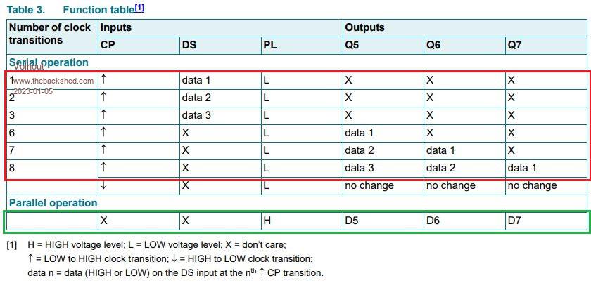 The red box shows the signals that must be controlled for shifting data - CP = Clock: the rising edge is shifting the next bit - PL = Load: a high level loads the input pins levels into the shift register, must be low now - Q7 = Serial Out: this is where the data is shifted out - DS = serial input. Will not be used in this example, so we connect to ground The green box shows how to load the 8 bit parallel data in the shift register. - PL = Load , must be high to load data. This analysis leads to the following connection diagram 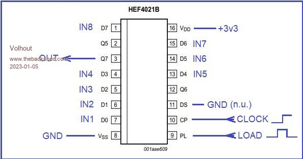 Now there is a lot in the datasheet in timing, and we can go to the detail in this, but that distracts for the moment. Let's skip it. Lets read the shift register. High level pseudo code: ' initialize PIO Pins 'label1: ' clear ISR ' set counter (X) to 7 ' generate load pulse 'label2: ' shift 1 bit in ' generate clock pulse ' decrement counter (X) ' when counter > 0 jump to label2 ' push ISR to FIFO 'we have read 8 bits (7....0) ' ' repeat (jmp to label1) The pseudo code above has no secrets for us. Let's assign pins to the PIO. For now let's connect clock to GP0, load to GP1, and read our serial data from GP2. We configure the pins in PINCTRL where SET has 2 pins (GP0,GP1), with base GP0. We shift IN from GP2, so the IN base is GP2. This is (PINCTRL 0,2,0,GP2,,GP0,) With this configuration the PIO program can be: 'address Ā Ācode Ā Āmnemonics Ā Ā comment ' Ā&h0 Ā ĀE083 Ā ĀSET pindirs 00011 set GP0, GP1 output ' Ā&h1 Ā Ā ĀE000 Ā ĀSET GP1=0 GP0=0 Ā Āinitialize clock and load low ' Ā&h2 Ā Ā Ā4060 Ā ĀIN NULL, 32 set ISR to 0 by shifting 32 NULL bits into it ' Ā&h3 Ā Ā E027 Ā ĀSET X=7 set counter to 7 ' Ā&h4 Ā Ā ĀE002 Ā ĀSET GP1=1 GP0=0 start load pulse ' Ā&h5 Ā Ā ĀE000 Ā ĀSET GP1=0 GP0=0 end load pulse ' Ā&h6 Ā Ā Ā4001 Ā ĀIN 1 bit shift in 1 bit from GP2 ' Ā&h7 Ā Ā ĀE001 Ā ĀSET GP1=0 GP0=1 start clock pulse ' Ā&h8 Ā Ā ĀE000 Ā ĀSET GP1=0 GP0=0 Ā Āend clock pulse ' Ā&h9 Ā Ā Ā0046 Ā ĀJMP X-- 6 decrement X and jump to 3 when X<>0 ' Ā&hA Ā Ā Ā8000 Ā ĀPUSH push the ISR value into FIFO (we have all 8bits now) ' Ā&hB Ā Ā Ā1F02 Ā ĀJMP 2, dly=31 restart the whole read cycle after 31 cycles delay (delay is just for fun....) When you run this code with the 8 inputs of the shift register not connected, you get following result (pins are undefined): 11001111000000000000000000000000 11111001000000000000000000000000 111110000000000000000000000000 11001111000000000000000000000000 11111001000000000000000000000000 10011110000000000000000000000000 11100111000000000000000000000000 The bits end up at the MSB of the 32 bit variable. We are shifting the data in from the wrong side. This can be adjusted in the SHIFTCTRL register. We have not discussed this before. SHIFTCTRL a,b,c,d,e,f a/ push threshold (leave 0 for now) b/ pull threshold (leave 0 for now) c/ autopush (leave 0 for now) d/ autopull (leave 0 for now) e/ IN-shiftdir (1 = shift MSB, 0 = shift LSB) f/ OUT-shiftdir (1 = shift MSB, 0 = shift LSB) So if we set e/ to 0 we get the correct shift direction. Since the others are not used no, we set all to 0 The below code is what results. We run the code at slow pace (100kHz) since the HEF4021 (CD4021) are slow devices. The maximum for these devices is around 2MHz at 3.3V. 'disconnect ARM from GP0/1/2 setpin gp0,pio1 Ā Ā Ā Ā 'clock setpin gp1,pio1 Ā Ā Ā Ā 'load setpin gp2,pio1 Ā Ā Ā Ā 'data in 'configure pio1 p=Pio(pinctrl 0,2,,gp2,,gp0,) Ā Ā Ā Ā 'GP0,GP1 out, GP2 IN f=1e5 Ā Ā Ā Ā Ā Ā Ā Ā Ā Ā Ā Ā Ā Ā Ā Ā '100kHz s=PIO(shiftctrl 0,0,0,0,0,0) Ā Ā Ā Ā Ā'shift in from LSB for IN (and OUT) 'address Ā Ācode Ā Āmnemonics Ā Ā comment ' Ā0 Ā ĀE083 Ā ĀSET pindirs 00011 set GP0, GP1 output ' Ā1 Ā Ā ĀE000 Ā ĀSET GP1=0 GP0=0 Ā Ā initialize clock and load low ' Ā2 Ā Ā4060 Ā ĀIN NULL, 32 Ā Ā Āset ISR to 0 by shifting 32 NULL bits into it ' Ā3 Ā ĀE027 Ā ĀSET X=7 Ā Ā Ā Āset counter to 7 ' Ā4 Ā Ā ĀE002 Ā ĀSET GP1=1 GP0=0 Ā Ā start load pulse ' Ā5 Ā Ā ĀE000 Ā ĀSET GP1=0 GP0=0 Ā Āend load pulse ' Ā6 Ā Ā Ā4001 Ā ĀIN 1 bit Ā Ā Ā Āshift in 1 bit from GP2 ' Ā7 Ā Ā ĀE001 Ā ĀSET GP1=0 GP0=1 Ā Āstart clock pulse ' Ā8 Ā Ā ĀE000 Ā ĀSET GP1=0 GP0=0 Ā Āend clock pulse ' Ā9 Ā Ā Ā0046 Ā ĀJMP X-- 6 Ā Ā Ādecrement X and jump to 3 when X<>0 ' ĀA Ā Ā Ā8000 Ā ĀPUSH Ā Ā Ā Ā Āpush the ISR value into FIFO (we have all 8bits now) ' ĀB Ā Ā Ā1F02 Ā ĀJMP 2, dly=31 Ā Ā Ārestart the whole read cycle after 31 cycles delay (delay is just for fun....) 'program pio1 pio program line 1,0,&hE083 pio program line 1,1,&hE000 pio program line 1,2,&h4060 pio program line 1,3,&hE027 pio program line 1,4,&hE002 pio program line 1,5,&hE000 pio program line 1,6,&h4001 pio program line 1,7,&hE001 pio program line 1,8,&hE000 pio program line 1,9,&h0046 pio program line 1,10,&h8000 pio program line 1,11,&h1F02 'write the configuration PIO init machine 1,0,f,p,,s,0 'start the pio1 code PIO start 1,0 'Check the the read data in MMBasic dim d% do Ā Āpio read 1,0,1,d% Ā Āprint bin$(d%) Ā Āpause 200 loop END The program will constantly poll the shift register, and when there is an empty slot in the FIFO, it will insert the data in it. Once every 200ms the MMBasic program pulls out a 32 bit word, and displays it. The CD4021/HEF4021 is the shift register that is used in the Ninendo NES controller. So the above code can be used to read the 8 buttons of a NES controller. That gives a practical flavour to this chapter. What is essential to a NES controller is that you always need the most actual value of the keys, not something that has been in a fifo for unknown time. This can be enforced by reading the whole fifo, and 1 value beyond the end. Below code shows how it is done... 'Check the the read data in MMBasic dim d%(4) do Ā Āpio read 1,0,5,d%() Ā Āprint bin$(d%(4)) Ā Āpause 200 loop We read 5 values from the fifo. The first 4 we ignore (they are old), the 5'th must be actual since it is just writen in the fifo. What if we would like to read a different shift register. This is the datasheet of the 74HC165. We go the same path.  this results in below connection diagram 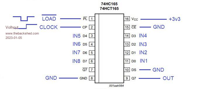 The difference with the 4021 is that the load puls is going low for load. During shift it is high. The first exercise is to adapt above program to support the 74HC165. If you happen to have a 74LS165, it must be powered from 5V. The clock and load inputs will accept 3.3V signals, but the serial output is 5V. A 1k/2.2k resitor divider will make a 3.3V signal for the picomite. The second exercise is to adapt the HEF4021 program to use SIDE SET for clock and load signals. This shrinks the program size significantly, and doubles the speed. Hint: all SET commands except the first (set pindirs) will disappear. Happy programming Edited 2023-01-05 06:37 by Volhout PicomiteVGA PETSCII ROBOTS |
||||
| The Back Shed's forum code is written, and hosted, in Australia. | © JAQ Software 2026 |
