| |
  Page 48 of 48 Page 48 of 48 |
| Author |
Message |
Revlac

Guru

Joined: 31/12/2016
Location: AustraliaPosts: 1307 |
| Posted: 11:57pm 24 Nov 2024 |
 Copy link to clipboard Copy link to clipboard |
 Print this post |
|
It would e easy to keep the output stepdown xformer. 
Cheers Aaron
Off The Grid |
| |
poida

Guru
Joined: 02/02/2017
Location: AustraliaPosts: 1485 |
| Posted: 06:49am 25 Jan 2026 |
Copy link to clipboard |
Print this post |
|
this note is examining the Vfb circuit that TinyT designed, that makes up
part of the nanoverter he created for us.
When I first looked at it, it seemed a bit too much for the job.
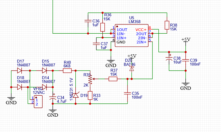
But it is all needed, to get the job done well and with protection
which is:
- take 12V AC and rectify it, via a full bridge diode layout
- smooth the result via a 4.7uF cap
- limit high voltage via a 5.1V zener
- give the user facility to adjust output voltage via a trimpot
- again smooth output, via a RC low pass filter
- limit low voltages to about -0.2V using a low forward voltage drop schottky diode
- feed this into a second order low pass active filter
- but first buffer it's input with a simple voltage follower
- the output is now cleaned of all nasty high frequency stuff
that would upset the closed loop control loop that manages the inverter output.
All this was easy to see back when I first saw it.
But I was always wanting to see how that active filter worked...
The filter is a Sallen-Key second order low pass filter.
It uses 2 caps and 2 resistors to define the filter.
In this case, both caps are 1uF and both resistors are 15K
3db cutoff is 1/(2xPIxCxR) or 10.6 Hz
The second order filter is nice, in that it attenuates output frequencies
10x for each doubling of frequency. or it's 20db per octave. same thing.
Once input noise that gets to 1kH the attenuation is very strong indeed.
It's perfect to get rid of the 20kH FET switching, and it's higher harmonics.
I made a simulation of the Vfb circuit. It runs in a free simulator you can download.
the simulator
here is the file you need to open from with the simulator app.
vfb sim.zip
unzip the app folder, run the program "circuitjs1.exe"
I have a simple input, 50Hz, and it's voltage can be abruptly changed via a switch. (just click on the switch)
The traces at the bottom show input into the active filter and it's output.
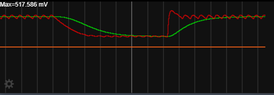
Red is the filter input, Green is it's output.
Technical analysis (way beyond my brain..) of the filter has shown it's transient response to be about 0.1 second and we can see the output get very close to the input voltage after about 0.1 seconds.
This speed of responding to input is fine. It permits me to design a closed loop control that will not go haywire and blow it's self to bits because it will
always have smoothly changing inputs thanks to the filter.
But it still has fast enough response too.
It has taken me a lot of words to say the thing I wanted to say in the first place, which is, TinyT you did a fantastic job designing the nanoverter and I remain grateful for your time and effort you put into this project.
wronger than a phone book full of wrong phone numbers |
| |
poida
Guru
Joined: 02/02/2017
Location: AustraliaPosts: 1485 |
| Posted: 01:51am 22 May 2026 |
Copy link to clipboard |
Print this post |
|
Looking at total system resistance in the primary winding + choke + FETs
The test inverter on the bench at the moment is my 4 x One HY5608 board,
using isolated gate drive optocouplers, with these supplied by 2 simple charge pumps.
Supply is 54.1V DC, on board control power is 14V, from a single dc-dc converter.
This drives a 40uH choke, into a 10.8:1 ratio primary that makes 235V AC output.
I was always wondering if I could measure the total system resistance and so, potentially get an idea of heat losses.
The code running my picoverter, as well as Wiseguy's inverter, displays the PWM width.
This measure is clock cycles, where fully on is 800 and fully off is zero.
the inverter with zero load needs a PWM width of 444
444/800 = 0.55
the DC-DC conversion ratio is 0.55
54.1 V x 0.55 = 29.75 V and this is the peak voltage of the AC wave in the primary.
0.707 x this is the AC voltage since it is nearly a Sine wave.
0.707 x 29.75 = 21.0 V
I put the Fluke 87 across the toroid's primary and I see 21.8V
near enough for me.
The AC current clamp meter says 1.6A with no load on the primary winding.
I place a 293 W load on the output. this load is light globes and fully resistive
with a power factor of 0.99
Now the AC current is 13.8A on the primary.
PWM becomes 464
DC supply current is 5.9A
We have enough info to work out the resistance of the total primary circuit.
R = V/I
I will not care about impedence here. But I should...
Volts is (464-444) / 800 x 54.1 = 1.35 V
Current is 13.8 - 1.6 ,sort of, and so it's = 12.2 A
R = 1.35/12.2 = 0.11 Ohm
from this I can get approximate inverter loss, ignoring many other things too
W = V*V/R = 16.5W
I wondered what might happen if I put a resistor in the primary circuit.
I used my 1 Ohm 3kW thing, and when in circuit and under load PWM became 742
idle PWM changed, increasing to 450.
so the primary circuit resistance can now be found from this data.
(742 - 450)/800 x 54.1 = 19.7 V
current remains at 12.2 A AC
19.7 /12.2 = 1.6 Ohms.
There is a long run of thin wire in the primary now so skin effect
likely reduces effective conductive area to a large degree.
There is a large amount of power in the 100kHz range running through
the primary circuit.
this is why it increased by 1.5 Ohms, not 1.0 Ohms
which I measured with a DVM so it's DC resistance.
power loss now becomes 19.7 x 19.7 / 1.6 = 242W
I noticed the DC supply increased from 5.9 A to 9.4 A at 54.1 V
and this increase in supply power is 189 W
this does not add up. it should be closer to the 258W
wronger than a phone book full of wrong phone numbers |
| |
KeepIS

Guru
Joined: 13/10/2014
Location: AustraliaPosts: 2268 |
| Posted: 10:11pm 22 May 2026 |
Copy link to clipboard |
Print this post |
|
The following observations may be of no use, but as you said, the skin effect in a thin wire will be considerable. In my testing, even at very low power levels just above idle, I could melt a thin lead in seconds from RF Skin effect during some "purposefully dodgy" choke testing on waveform distortions and circuit changes, perhaps the loss is even more than anticipated?
Obviously, the other thing that became apparent, due to skin effect, was the very real and increased Loss / Heat in the Choke, Toriod and Power board terminations in the primary side circuit (SPWM Drive), requiring extra effort (a lot) to ensure near perfect crimping of all terminations and all terminal connections, washers, screws, surface flatness, etc.
I find the thoughts and testing ideas that you come up with very interesting, I wish I had more time to do some of it, but in the meantime, it's great to read and follow along.
NANO:Inverter V 8.4ks - Linux AvrDude GUI script V4.1 |
| |
| |
Page 48 of 48 |

 Notice. New forum software under development. It's going to miss a few functions and look a bit ugly for a while, but I'm working on it full time now as the old forum was too unstable. Couple days, all good. If you notice any issues, please contact me.