
|
|
Forum Index : Electronics : Various aspects of home brew inverters
| Author | Message | ||||
Madness Guru Joined: 08/10/2011 Location: AustraliaPosts: 2498 |
The glossy paper is the type used to get nice colour laser prints, the gloss is actually polished clay same as glossy magazines. Usually they call it Gloss Color copy paper, it is not ink jet photo paper. It can be bought at your bigger office supply stores in A4 quite easily, I also use A3 for my power pcb's to get full coverage of the 200 X 300mm board, the A3 is much harder to find. I have found the surface scratching does give far better adhesion, the amount of copper lost is very minimal. As for question 2, I do exactly as you have quoted, only thing I have found is that if it is too hot the toner will start to spread under the pressure of the laminator rollers. I use a Kyocera colour printer/copier, other machines with different toner may have different temperature requirements. If you wanted to after drilling the PCB you could print a silkscreen and transfer it on the same way, I have found it to be fairly robust but will scratch if anything sharp comes in contact with it. I have had no issue at all using Acetone on PCB's, is quick and removes the toner with very little effort. After drilling I use Oztules tip and spray lightly with Lanox and wipe with a cloth, it prevents oxidisation and aids soldering. If you put it on prior to drilling it makes the drill shavings stick to the PCB. There are only 10 types of people in the world: those who understand binary, and those who don't. |
||||
| Tinker Guru Joined: 07/11/2007 Location: AustraliaPosts: 1904 |
Thanks for the tips Gary, I will look out for that gloss paper next time I go to Officeworks. I'm also in the market for a cheap laser printer. By cheap I mean ~$50.- The Samsung laser printer I used so far has run out of toner and a new cartridge (if I can find one) costs way more than a new printer. Its the only job I do with a laser printer so no point to get an expensive one. I use an inkjet for all other printing. Unfortunately the only cheap laser printers locally seem to be the Brother brand and I have been told their toner is not very good for PCB transfer. The Samsung toner worked fine, I might have to look on ebay for a printer. Klaus |
||||
| poida Guru Joined: 02/02/2017 Location: AustraliaPosts: 1476 |
This is growing to be a good topic. I think we needed one where we can talk about details of this and that. I hated potentially derailing other's posts. Part 4: Closely watched mosfet gate voltages I have been interested in what is happening to the mosfet gate when switching on and off. Some test setup facts, first. Mosfets are IRF3808, 3 per leg of the bridge. gate drive ICs are IR21844 1/2 bridge rated at 1.4A source current, 1.8A sink current. The outputs of the driver chips have 4.3 Ohm gate resistors in series, 10K pull down and 1N4148 diodes in parallel with the 4.3 Ohm resistors. Only a couple of DSO traces this time. 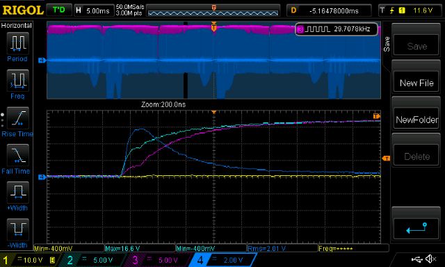 This shows the low side 20kHz mosfet switch ON event. Light blue is voltage on driver side of the 4.3R resistor Purple is the mosfet side of the 4.3R resistor. Blue is the differential voltage across the 4.3R. The peak voltage drop across 4.3R is not quite 6V. This corresponds to a peak current of 6V/4.3R = 1.4A So far so good, The driver IC can only source 1.4A from the specs. so it seems that for a little period the driver IC is in some constant current mode. Or maybe the gate drive resistor value was chosen well so that the 1.4A max is not exceeded. Next, I can see the plateau in Vgs when it attains Vgs-threshhold. Specs say it's 2 to 4V, use the purple trace to see this, it is the mosfet gate voltage, not the driver IC output. I read about this multi-stage Vgs behavior from many sources but here it is. It seems to plateau out for about 40ns. Finally, looking at the blue trace, it appears to me to be just as if we were charging a capacitor. (we really are when switching a mosfet..) Anyway, it's really nice to see this in Real Life(tm) Your thoughts on this? Just to see if I am on the right planet, let's work out the capacitance at a particular point in time - right after the purple trace plateau finishes and it rises nearly linearly. Let C (capacitance) = Current x time / voltage change (this is the same thing as the Inductance formula I used earlier in this topic.) I will use 1.4A for current which I will make it remain constant for the below calcs. 2 ticks of the 200ns time div, or 80ns voltage rise will be something like 4 ticks of the 5V, or 4V so C = (1.4 x 80E-9)/4 = 28nF I'm probably making a stupid error here but when I look at 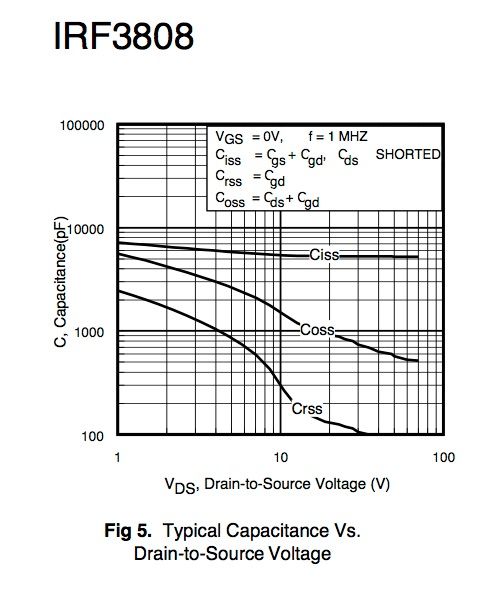 It seems to make sense. The drain to source voltage is the inverter supply and it's approx 30V. Here is the switch OFF event, same trace legend as above. 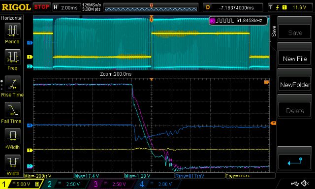 The blue trace is negative now, the gate drive IC is now sinking current, with a max sink of about -0.46 A It seems we can drive the gate down faster, the drive IC is rated at 1.8A sink. I wonder if the 1N4148 is limiting the sink current? Anyway, the whole point of this is show to myself that what we are doing is charging and discharging a capacitor when switching a mosfet. I find it necessary to see for myself rather than simply read what it is from textbooks. And this has lead me to the next question: what is going on with the 1N4148 diode during mosfet turn OFF. Is there a big voltage drop across it? Or maybe it has a slow reverse recovery time. Are these diodes needed? Could I use faster ones or those with less forward voltage drop? wronger than a phone book full of wrong phone numbers |
||||
Revlac Guru Joined: 31/12/2016 Location: AustraliaPosts: 1276 |
Thanks for the conformation Warpspeed that zener should help as a safety measure. The Chinese can make good stuff, a friend from china once told me, you can buy an electric motor for a drill press you can have a cheap one or an expensive one all look the same, the expensive one is built in a factory the other is built in someones basement, that was years ago. The fets i had Magnachip were made in china, the new lot just arrived made in south Korea. Tinker the method that Gary used for pcb transfer works really well, The brother laser printers don't have good toner, I had to heat it until paper went a little brown, no smudges a sticks well Poida mentioned some simulation software? in an earlier post. I have not found any free software that is useful yet or had the time. Aha thats good Poida its nice to see the switching in action,I do wonder what effect that fast turnoff has on transformer side. though the 3808 seems to handle the speed. I will read this again tomorrow. Cheers Aaron Off The Grid |
||||
| Warpspeed Guru Joined: 09/08/2007 Location: AustraliaPosts: 4406 |
Its nice to have good test equipment and actually be able to test and measure things. There is no real way to know for sure what is happening unless we can see it. My poor old oscilloscope was developing new faults faster than I could fix old faults, and I eventually gave up on it. So bit the bullet and bought TWO more oscilloscopes, a fast analog scope and a digital scope. Have not really used the digital scope yet for anything serious. But those gate switching waveforms above are pretty exciting. And impossible to see on anything but a digital storage scope. Cheers, �Tony. |
||||
| poida Guru Joined: 02/02/2017 Location: AustraliaPosts: 1476 |
a google search "multisim torrent" gives a link going to radiouniverse That is v14 and may be useful for a bit of a play. another search "multisim 11 torrent" gives a link to google docs. This also might work for you. Since these are hacked/cracked they probably bring some risk of computer damage so use at your own risk, etc. wronger than a phone book full of wrong phone numbers |
||||
| poida Guru Joined: 02/02/2017 Location: AustraliaPosts: 1476 |
Warpspeed, which oscilloscopes did you buy? wronger than a phone book full of wrong phone numbers |
||||
| Warpspeed Guru Joined: 09/08/2007 Location: AustraliaPosts: 4406 |
Digital is a Tektronix 2430 the first digital Tektronix ever made, and one of the very first digital oscilloscopes on the market. Analg scope is a Tektronix 2445B, four channel 200 Mhz its the last analog oscilloscope they ever made and arguably the best. They are both from about the same era, mid to late 1980's so they are both now quite old. But both are in excellent condition and well worth the few hundred dollars each cost. They are also the last Tektronix oscilloscopes you can get full service and repair manuals for, or spare parts. All the later stuff now is essentially unrepairable. Cheers, �Tony. |
||||
| Solar Mike Guru Joined: 08/02/2015 Location: New ZealandPosts: 1212 |
Very interesting, I like your detailed scope examination. When we parallel many mosfets, eg 6 per leg of the bridge, I think your scope would show a different story. The typical IRFP4110BPF has a combined gate charge of 180nC, so 6 paralleled have a combined charge of 1080nC. The typical driver chip IR2110 can only supply 1.6 amps, but as it has to drive 6 devices then the max drive current per device for even current sharing is 1.6/6 = 0.267 amps, so the mosfet turn on time is now Q/I = 180nS/ 0.267 = 674 nSec, a lot more. In this case the gate resistor should be approx 40 ohms not the normal 5.6, ie 12v/0.267a, to prevent damage to the driver. With this driver chip if the resistor was made smaller then not all mosfets would turn on evenly as the driver cannot source enough current, so some mosfets will draw more current than others and perhaps self destruct in doing so. If a diode is paralled with the resistor, normally this has the effect of discharging the gate charge quicker, assuming the driver can sink the increased current spikes without blowing up. A small fast signal switching diode is normally adequate, but when using totem pole drivers its not really required, the Bridge driver should have a sufficient dead time period. If a gruntier driver is used eg TC4452, with a 13amp peak, then our 6 mosfets could be supplied each with 2 amps, requiring a gate resistor of approx 5.6 ohms, the turn on time 180/2 = 90 nS, much better. We dont want too fast a turn on of course as this can lead to device dv\dt avalanche breakdown or severe ringing waveforms, causing voltage spikes to exceed drain source limit. When higher power fets are used, currently I'm using IRFP4468, these each have a gate charge of 400nC so its essential something like a TC4452 is used when 4 or so are paralled together. Cheers Mike |
||||
| poida Guru Joined: 02/02/2017 Location: AustraliaPosts: 1476 |
Thanks Mike for the comments. I am struggling to quantitatively work with the gate capacitance and available current. I could not get my head around the gate charge/current/time thing. Thanks for the examples. I will look at my prototype and see if it makes sense. Additionally, when you write "..In this case the gate resistor should be approx 40 ohms not the normal 5.6, ie 12v/0.267a, to prevent damage to the driver. With this driver chip if the resistor was made smaller then not all mosfets would turn on evenly as the driver cannot source enough current, so some mosfets will draw more current than others and perhaps self destruct in doing so." I cant help but think of Tinker's woes. Maybe a good approach to inverter design would be: 1 select matched FETS, tested as good and well suited for parallel use 2 figure out the gate charge and driver current needed to get sensible switch speeds 3 verify adequate dead time 4 verify ringing on gate or drain or source is small enough to live with 5 ensure little or no dV/dT turn-on, and other parasitic issues Once these are sorted, only silly overload mistakes should kill the mosfets. What other failure modes are there? No 3,4 and 5 will need a decent digital storage oscilloscope. wronger than a phone book full of wrong phone numbers |
||||
| Tinker Guru Joined: 07/11/2007 Location: AustraliaPosts: 1904 |
Yeah right, but we don't have a decent digital storage CRO. And, buying an off the shelf inverter might turn out to be cheaper  So it's left to experimenting, at least for this tinkerer. I could blow up an awful lot of Mosfets for the price of that fancy scope. Thanks for the gate resistor thing, I try to experiment with that for a bit. Not bored with it yet but have to slow down a bit to catch up with neglected house chores  Klaus |
||||
oztules Guru Joined: 26/07/2007 Location: AustraliaPosts: 1686 |
My observations are like this. I originally used a power jack main board, and it had 50R resistors on the gates, and no diodes. Worked fine with the PJ drivers, but the 8010 using the 2110 blew up very quickly...... would run for a bit, but heat up very very fast. So went to 5ohms, and the heat disappeared, and suddenly everything worked perfectly. When you can drive it up to 20kw to start big motors, you no longer worry about the drive. You can drive it all day at 4kw, and it does not care, with excursions to 8kw and back.... still runs fine. Mad has had very good success with SOME of his tests, and has driven 8kw for long times I would not believe..... other times he has self destructed quickly, and at low loads. Torroids take no prisoners, and this aspect is the most important I think, any tiny frequency drift, or loss of a wave form for any reason ( somehow turning off the 2110 for an instant) will kill the fets dead in one cycle. I have had one unit die from idling for a few days, then dumping the house load on it. It had done a few MWH under harsh loading, but the idle seemed to be the killer. It idled for days, then at the first sign of load, blew up instantly.... could be the transfer switch too...... This does not look like a driver problem, but a back emf problem, between the chip logic and the load change after a long time doing nothing. This may never have happened if it was a E-I tranny.... or was it the transfer switch??? There are quite a few of these running happily driving houses around here with no sign of trouble.... but I do still wonder why the thing died on idle, and yet none have ever had problems at high power... they lap it up. So I dont know why ... if the driver is so badly out of whack @ 5R, why it works fine so far. I don't understand how tinker has had such a poor run... yes he has unorthodox layouts, but my experience so far has been that these things are pretty forgiving... if they work for me they should work for anyone..... and I have run these things hard for days with them spread out all over the place on the bench. The drive info is salient, but I feel it is something else altogether. The 10pn connector has very thin wire in there, and that will drop the current too. The chinese boards using the egs002 boards have very low R in their gates too..... some just tie the gates together, and run a single 5r resistor... they still work just fine.. It just does not seem to be critical, much as the theory says it is. I'm just not convinced so far. oztules Village idiot...or... just another hack out of his depth |
||||
| Madness Guru Joined: 08/10/2011 Location: AustraliaPosts: 2498 |
Has anybody seen details of the 7500W Chinese Inverters that have 2 extra MOSFETs in the gate drive circuits as shown here .  There are only 10 types of people in the world: those who understand binary, and those who don't. |
||||
| Warpspeed Guru Joined: 09/08/2007 Location: AustraliaPosts: 4406 |
One thing that needs mentioning is that there are three totally different types of drive waveforms used to drive bridge type inverters with pwm, and that can make quite a difference. The Power Jacks appear to drive the upper two mosfets with only a 50 Hz square wave, so the upper pair turn on alternately at only 50 Hz. Then only one of the lower drive mosfets is PWM'd and the other lower mosfet remains off for half a cycle. I have never had a Power Jack to play with myself, so am not absolutely certain of that but it is a perfectly valid way to do it. A second way to do it is to drive a diagonal pair together, where one diagonal pair is PWM'd for half a cycle, and then is turned fully off for the other half cycle. A third way to do it is to drive all four mosfets continuously with pwm, but have the duty cycle of all of them hit 50% together at the zero crossing points. There are all kinds of advantages and disadvantages with each each of these methods. I rather gather that the 8010 board continuously PWMs all four mosfets, so its fundamentally very different to the Power Jack. Cheers, �Tony. |
||||
| Solar Mike Guru Joined: 08/02/2015 Location: New ZealandPosts: 1212 |
Well theory goes out the window sometimes in the real world when other factors come into play, there are many combinations of builds that are out there, slightly different transformers, different layouts, suspect quality of some Chinese sourced components; these no doubt all have an effect. >> Has anybody seen details of the 7500W Chinese Inverters that have 2 extra MOSFETs in the gate drive circuits as shown here . Yes they are TIP41C and TIP42C transistors driven by the IR2110 as a totem pole complementary pair, I have one of those boards, will see if I can trace out their circuit connection. Great idea placing them close to the driven mosfets. Cheers Mike |
||||
| oztules Guru Joined: 26/07/2007 Location: AustraliaPosts: 1686 |
I'm pretty sure my original W7 was unipolar. I run the 8010 unipolar too. The more recent PJ boards I have seen have been bipolar.... I thought they were unipolar too. The 8010 can run either way as well. ( jumper)... like this. 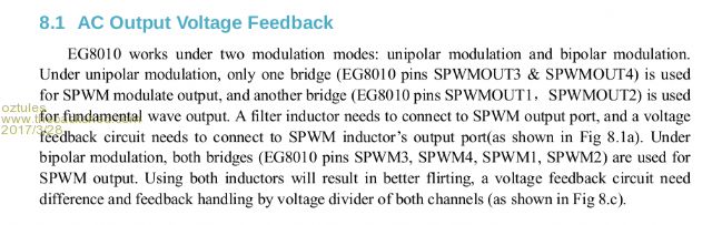 ........oztules Edit Solarmike, I would very much like to see your diagram..... it makes sense, and leaves the drivers native. Village idiot...or... just another hack out of his depth |
||||
| Madness Guru Joined: 08/10/2011 Location: AustraliaPosts: 2498 |
Thanks Mike I would really appreciate the gate circuit. While I have no doubt about Oztules success I just can't replicate it, I have built probably 8 or 9 power pcb's with various changes all aimed at matching the design of the chinese boards and blown up over to 200 FETs. So far I have not been able to build an Inverter with more than 12 MOSFETs that produces a clean waveform with no spikes. I have got close with 24 MOSFETs, but best I have done is 10 days running the house. Maybe I just don't have the right DNA to make it work. There are only 10 types of people in the world: those who understand binary, and those who don't. |
||||
| Warpspeed Guru Joined: 09/08/2007 Location: AustraliaPosts: 4406 |
Just trying to shine a bit of light into a rather dark place, but another thing to think seriously about is driving capacitive loads. The large magic toroid is a wonderful thing, it reflects back anything connected to the secondary straight back into the primary. And that includes any capacitance across the secondary winding, either deliberately added, or what natural capacitance is normally there between the actual secondary turns and the steel toroid. The natural self resonant frequency of the secondary is very likely to be well below 20 Khz, the bridge will then be driving a highly capacitive load, even if there is nothing else connected to the secondary. Its also fairly common to connect a large capacitor directly across the secondary to filter out the 20 Khz pwm. That produces a lovely clean sine wave, but it is really going to stress out your mosfets every time they switch. To make the problem even worse, fitting a bunch of large electrolytics across the incoming dc supply to the bridge only increases the current spike during each switching cycle. There absolutely must be sufficient inductance somewhere to limit the rate of current rise during switching. The ferrite core in series with the primary is an excellent way to limit the initial rate of current rise under no load, but it will very quickly saturate. There is really no substitute for having a decent oscilloscope and monitoring all the voltage and current waveforms. The bridge itself may be working fine with reasonable speed and sufficient dead time, but what that bridge has to drive can have a significant effect on the switching stress. Cheers, �Tony. |
||||
| oztules Guru Joined: 26/07/2007 Location: AustraliaPosts: 1686 |
Even here these things seem to not care. There are a few of these here that run 150uf or more driving a 2.5kw hot water element during the 10-4 time slot. They don't seem to have any effect on the units.... they run them just perfectly. This allows the hot water element to run at say 1kw, and the battery only sees this.... the inverter sees the power factor problem and has more VA than the load... but the battery only see the watts...... but the huge capacitance seems to be of no conern at all. It's all a mystery as to why it works so well, but cap loads don't seem a bother at all for even long periods. Mad, the ones with 12 fets that had a good wave form... how did they survive. .........oztules Village idiot...or... just another hack out of his depth |
||||
| Madness Guru Joined: 08/10/2011 Location: AustraliaPosts: 2498 |
I have not run them for long as yet but I am planning to do that very soon and see how the survive. I won't run the AC off it so should not get over 4KW load. There are only 10 types of people in the world: those who understand binary, and those who don't. |
||||
| The Back Shed's forum code is written, and hosted, in Australia. | © JAQ Software 2026 |
