
|
|
Forum Index : Electronics : Various aspects of home brew inverters
| Author | Message | ||||
mackoffgrid Guru Joined: 13/03/2017 Location: AustraliaPosts: 460 |
I'm going to assemble a discrete circuit, if only as a test. But this part looks to be designed for the job. ZXGD3005 No idea where to get them though. Cheers Andrew |
||||
| poida Guru Joined: 02/02/2017 Location: AustraliaPosts: 1480 |
You are a pioneer with this. I have wondered if doing this would be a complete solution to the induced gate voltages. I am keen to see how you go with this. The timing for those switches will need to be closely coordinated with the main MOSFET gate signalling. I wonder if dv/dt induced gate voltages when clamped by the extra FETs will still be present within the main bridge MOSFETs and so we still see shoot through... That is, pulling down the Gate to Source is never enough. wronger than a phone book full of wrong phone numbers |
||||
| poida Guru Joined: 02/02/2017 Location: AustraliaPosts: 1480 |
Digikey has them wronger than a phone book full of wrong phone numbers |
||||
| wiseguy Guru Joined: 21/06/2018 Location: AustraliaPosts: 1297 |
Thanks Andrew - I learn't something today, must admit Spirito sounded a bit like voodoo stuff but I googled it and it is real ! I know well about linear planar versus trench when wanting linear performance but although this "Spirito" effect is closely aligned I had never heard of the gentleman or the effect named after him until your post. Do you have any figures from your tests; "dvdt can cause minor shoot-through at quite slow changes in Vdrain" With regards to the slew rate (rise time) when you noticed the effect, just wondering how slow "slow" was. A good description of gate resistor choice and some CRO shots are at this Link His conclusion about decent Gate drivers and low gate resistance concurs with these latest posts. Note his third picture is headed " 1V, to the gate, with a 1 Ohm load resistor" - I believe he meant to say "1V, to the Drain, with a 1 Ohm load resistor"- then it made more sense. We are not operating at 300V but the large Cgd of our Mosfets and with multiple units in parallel has a similar effect at 48V with respect to gate drive requirements. The post has moved on while I was writing this - there are drivers for IGBT's that have the negative offset you are after. I bought 10 of the ZXGD3005's but when I saw their size I abandoned them for the TC4452 after I was reminded how small a SOT26 is. If you want 2, PM your address and Ill send them over. If at first you dont succeed, I suggest you avoid sky diving.... Cheers Mike |
||||
| mackoffgrid Guru Joined: 13/03/2017 Location: AustraliaPosts: 460 |
Thankyou Mike I'm not sure how I will solder to them in my prototype but I'll give it a try. Yes, the TC4452 are far better and easier (under normal circumstances). I'm not sure what scope shots I have that would be useful, I'll be a few days before I have another go. Cheers Andrew |
||||
| wiseguy Guru Joined: 21/06/2018 Location: AustraliaPosts: 1297 |
Ill try to get them off tomorrow - get your magnifying glass ready..... I am sure you can read a datasheet - but don't overlook that they appear to be a glorified complimentary emitter follower and despite their claims that they can buffer output from a controller to a FET gate, this may be misleading. My understanding is that the gate drive voltage will always be the same as the signal input. If they are powered from 15V but the drive signal is 5V the output will only be ~5V. They can definitely buffer a 10-15V gate drive directly from an IRF2010 or similar though. If at first you dont succeed, I suggest you avoid sky diving.... Cheers Mike |
||||
| mackoffgrid Guru Joined: 13/03/2017 Location: AustraliaPosts: 460 |
It will be a challenge, I use a maggie lamp just to do through hole soldering these days. Yes, I was gleaning that (a glorified emitter follower) as I read you comment. Unimpressive for most jobs, but it seems cool how it can drive down to -Vee even though the input signal doesn't. We'll see. Thanks Andrew |
||||
| wiseguy Guru Joined: 21/06/2018 Location: AustraliaPosts: 1297 |
Be cautious, on page 4 bottom LHS & page 6 bottom RHS, the only -5V output pictures both show the input as being -5 drive. I am really a bit unimpressed with their misleading data sheet where we seem to have to crowbar out the relevant detail. Do you still want the parts  If at first you dont succeed, I suggest you avoid sky diving.... Cheers Mike |
||||
| mackoffgrid Guru Joined: 13/03/2017 Location: AustraliaPosts: 460 |
Hmmm, you're right. Looks like waste of time. Yea, hold off sending the parts. Thanks for having my back. You've saved us both the time. |
||||
| poida Guru Joined: 02/02/2017 Location: AustraliaPosts: 1480 |
Part 27: Why we make them big and beefy. (Inverters, that is) In earlier post here, I showed that my house needs a relatively low power supply for most of the day. I chose to supply this low level with the solar power system and let the high power loads be supplied by the street supply. This has enabled me to supply about 50% of the house power from the solar array over the entire year. This is Melbourne. Cloudy, overcast Melbourne. I see we only need about 5 to 10A at 50V for most of the time, then we only need an inverter that can handle 500W. Right? I have 2 fridges on the solar supplied circuit. When a fridge switches on due to it's thermostat, there are large current peaks. How large? This is the recorded data from my system. Green line is the smoothed or average current drawn by the inverter. Brown is the peak current seen at any time. We can see my house needs less than 10A most of the time, but very often, the inverter has to handle 50 A peaks when a fridge turns on. That is why we build inverter boards that can deal with 2 or 3kVA or more when running modest loads. First, today where quite modest power levels were provided by the inverter. 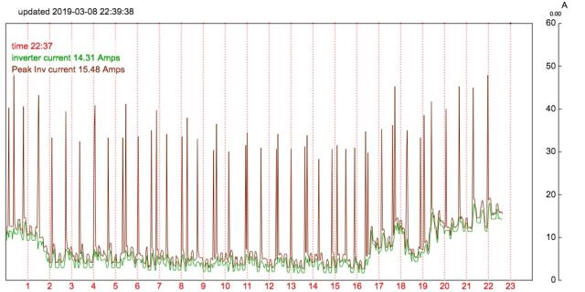 And last weekend, when I ran the pool pump. On top of this load, we can see the fridges peaks when they switched on. 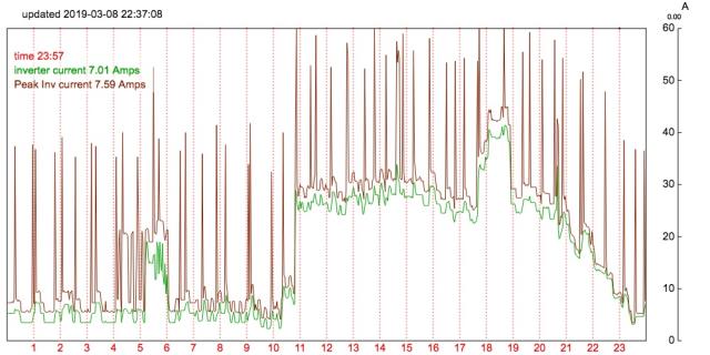 Over building the inverter is a good idea. The PWM based systems can run at quite high efficiencies under low loads. In my case the 250W to about 500W is at about 93% efficiency. This means at worst I waste 7% of 500W or 35W in heat. No fans need to come on to cool things. The reason the brown and green curves don't align at low power levels is that the current sensor has a lot of noise. The green curve is time averaged current, suppressing the noise effectively, the brown curve is recording the peak value seen at about a 1000Hz sample rate. wronger than a phone book full of wrong phone numbers |
||||
| poida Guru Joined: 02/02/2017 Location: AustraliaPosts: 1480 |
Part 28: Gate drive on Madness's power board. This uses on board transistor totem pole drive After building one of Madness's boards, I wanted to see the high and low side gate drive, focusing in particular on any signs of shoot through. Here are the results. Oscilloscope probe technique is important and I examine this later in the post. I look at gate drive voltages at 2 portions of the AC output sinewave just as I did in post #26 Looking at some location quite early in the 1/2 sine wave, we see high side switch ON and high side switch OFF. There seems to be a small degree of shoot through, the HY4008 specs say Vgs(th) can be as low as 2V and up to 4V. We see peaks well past 2V, into maybe 2.4V. I call this as getting to conduction on the low side MOSFETs during a high side switch ON event. This is far less severe than what I show in post #26. Yellow is LOW side gate drive Blue is HIGH side gate drive. I forgot to reset the probe gain in some of these. It is either 20x or 200x. 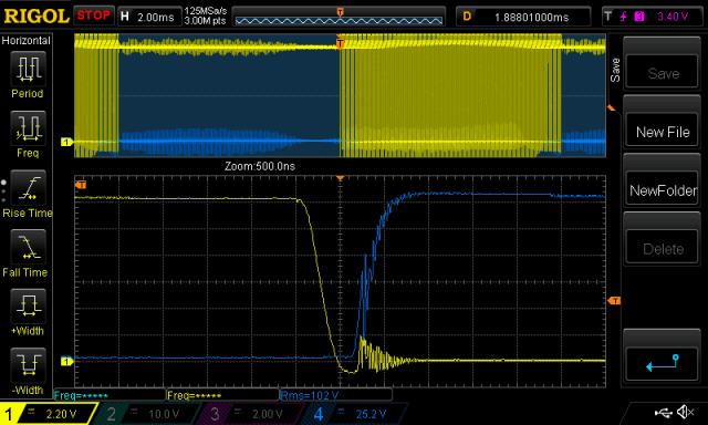 and 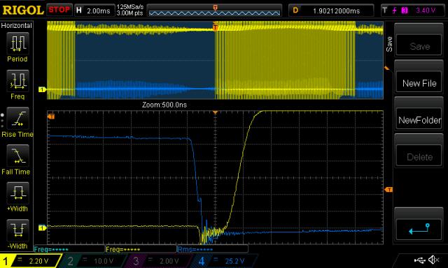 These following 2 are late in the same 1/2 sine wave of the AC output. Less issues to my eyes and again we can see a clear effect of dv/dt on the low side gate. It can be drive negative just as easily as it can be driven positive. 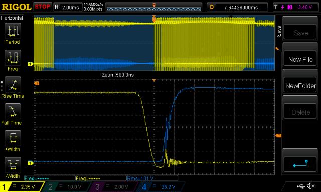 and 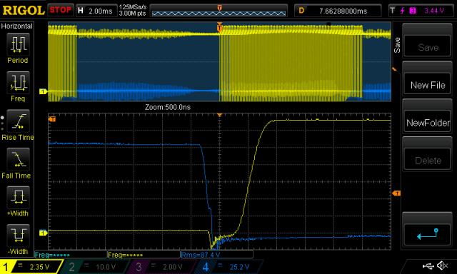 Some of the high frequency oscillations we can see everywhere are real. And some are due to the probe technique I used. I use the short 5 inch long alligator clip earth leads nearly every time. I used them in the above DSO traces. These short earth leads are an inductor and they create high frequency oscillation due to the approx 15-20pF capacitance of the probe and other parasitics combining to make an LC tank. Better probe tech. is to not use the earth lead. See how I do it. (only good for LOW side gate probing) I solder two small wires on both ends of the 20K gate to Source pull down resistor. I then poke the probe in these two springs. This is a very good way to minimise to a large degree the effect of the 5" earth leads. 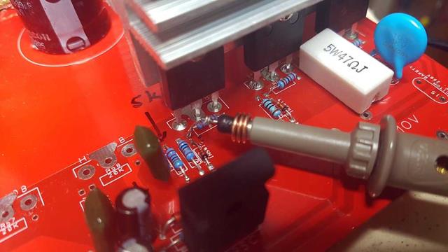 Let's look at a LOW side switch off and on event with this probe tech. First that near the start of the 1/2 sine wave 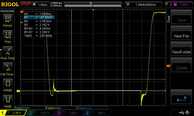 and that near the end of the 1/2 sine wave 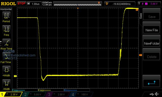 Zooming in to the right hand side rise event we see some oscillation, at about 6MHz  I feel this could be improved, no idea how. The value in reducing this is the MOSFET's could spend less time in the switching stage and more time either fully on or fully off. This will reduce heat, stress, increase inverter life and improve overall efficiency In case you think this is some poor DSO interpolation artifact, here are the data points at each sample time. 500MHz sample rate. 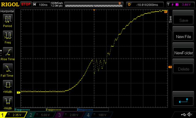 Yeah, yeah, probe compensation. I could/should do that and calibrate things and rent special test gear and, and... I need to show you other comparisons of with and without the little earth lead. Most striking is to do this on a digital output pin on an Arduino or Raspberry Pi or STM32 or something. It's night and day. Finally, a capture showing the gate voltage behaviour during a few PWM cycles. We can see the peak gate voltage sag a little but this can't be any problem. 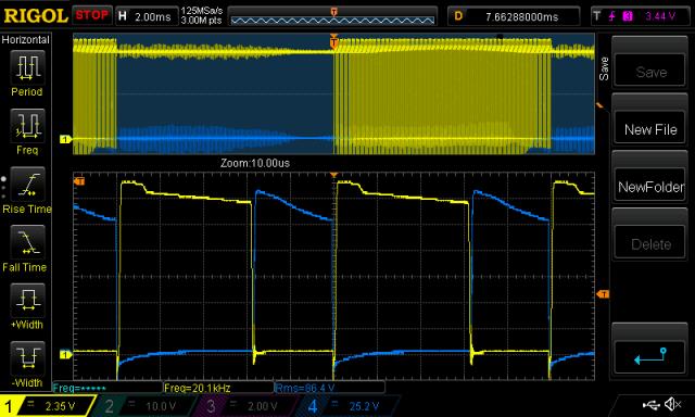 It is hardly surprising Madness's power boards work so well. They reduce, by quite a lot, the shoot through I see in power boards using IR2110 gate drive ICs directly to power MOSFET gates (e.g. Alliexpress inverter boards, Ozinverter designs, etc.) Wiseguy has some alternate power board designs in progress and I look forward to seeing how his go. They use closely located drive ICs and opto couplers. Maybe these will reduce even more the dv/dt effects? I may be repeating myself here but I must say: This is fun. wronger than a phone book full of wrong phone numbers |
||||
| wiseguy Guru Joined: 21/06/2018 Location: AustraliaPosts: 1297 |
Hi Poida, good to see you having so much fun. Today I received my digikey order with the opto-fet drivers etc so in the near future I will glue some bits onto a PCB make sure it works ok and send some stuff over for you to play with. Not really looking forward to fitting the smd parts though, thats the payback for being stingy & fitting too much on a small PCB..... I should also get my control PCB back hopefully within the week so I will populate some bits on that too including the bits for isolated supplies. It uses a synchronous sample and hold I codged up which holds the peak value of the output each half cycle of AC until you have read it after the zero cross. I incorporated 2 types of LED opto drive for the power stages from the Nano1, either IR2184s or a quad exclusive or gate. The exclusive or gate is meant to drive the optos for the top and bottom half bridges in inverse parallel as per Warps anti crossover/deadtime method. If using the 2184s they can just drive the optos separately as the 2184's have deadtime built in. The changeover from inverse parallel to separate is achieved with 4 x pluggable links. (the exclusive nor is a lot cheaper than 2 x 2184's so will be interesting too see the outcome) I also have a triple toroidal hiflux choke ~ 80uH that laughs at 70A I havent been able to saturate it yet but will find its limit soon, it is considerably better than the overgrown gapped ferrite E cores I have also been playing with, Ill send that too. I havent got any batteries or a decent toroid wound yet so in sending some stuff to you, at least I wont have to sweep up any charred plastic bits or clear the smoke from my shed  If at first you dont succeed, I suggest you avoid sky diving.... Cheers Mike |
||||
| Warpspeed Guru Joined: 09/08/2007 Location: AustraliaPosts: 4406 |
Poida, Back in the old days when very large IGBTs were pretty slow to turn off, it was quite common to use bipolar gate drivers that used +15v for gate turn on, and drove the gate a fair way negative to turn the IGBT off faster, and prevent spurious turn on from dv/dt in the lower device. https://www.fujielectric.com/products/semiconductor/model/igbt/application/box/doc/pdf/REH984e/REH984e_07.pdf Cheers, ĀTony. |
||||
| ltopower Regular Member Joined: 08/03/2019 Location: United KingdomPosts: 64 |
Poida, brilliant work with the scope. It's amazing to see the waveforms with 500MHz sample rate as they really do show up everything that is otherwise missed qyuite easily. I'm still scratching my head reading through some of it.. brilliant stuff. I read a while back in various posts about a UPS style version board and found it on Aliexpress, wondering if two units given a common stabilised input frequency if they would syncronise enough together to allow the two transformer outputs to be coupled. Small variations in the frequency lock may well create some degree of oscillation ? 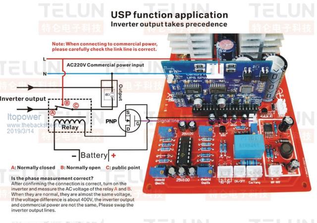 This would then allow an incremental build out of a larger inverter capacity.. this would also avoid them from actually being used as a UPS just a syncronised group of boards.. This is my inverter board that turned up today.... in need of some more solder on some of the drain and source legs..... 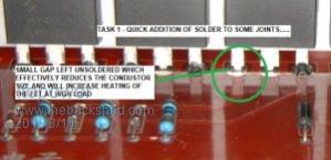 The effect of this small difference to FET leg position and heating effect would be quite interesting to know, although not entirely sure how this could be measured effectively. Maybe a comparison between two FET's as I noticed your picture with the scope leads the drain and source are in a similar low solder situation ? |
||||
| ltopower Regular Member Joined: 08/03/2019 Location: United KingdomPosts: 64 |
Ah, picture did not come out as planned... 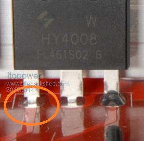 |
||||
| ltopower Regular Member Joined: 08/03/2019 Location: United KingdomPosts: 64 |
Just noticed that image is with the gate lacking in solder, there are other FET's on the board with the source leg in the same situation and wondering abut the heating impact of that very short narrowing of the leg. |
||||
| Solar Mike Guru Joined: 08/02/2015 Location: New ZealandPosts: 1228 |
Great work there Poida. To minimize the HF gate oscillations try placing a ferrite bead over each of the mosfet gate leads, or use a smd ferrite bead on the pcb at the gate connection, high current ones are available from element14 #2292371 that will handle the 8amp drive current pulses. Better yet is to have a totem pole buffer driver on each mosfet, this achieves better off signal clamping and helps prevent any shoot through, I use the ZXGD3005, they are only 50c each, need a magnifying glass to solder them though.. Cheers Mike |
||||
| Tinker Guru Joined: 07/11/2007 Location: AustraliaPosts: 1904 |
Ideally the middle leg (drain) would not carry any current, it instead flows via the heat sink to the back plane of the HY4008 - this connects to the drain. That is one reason for using life heat sinks and *no* heat sink compound at the mosfets. The source leg needs to carry the full current and I see in the pic a build up of solder for that, not sure if the PCB tracks are adequate. Klaus |
||||
| ltopower Regular Member Joined: 08/03/2019 Location: United KingdomPosts: 64 |
Appologies, that picture was not the best example... showed the extreme potential from a lack of solder. This is the other side of the board. 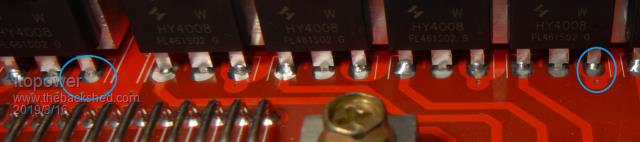 My thought is that this would be one source of additional heat generation.. I'm presuming it is the wider section of the legs that are part of the package constraint on the amps rating ? |
||||
| Warpspeed Guru Joined: 09/08/2007 Location: AustraliaPosts: 4406 |
Don't forget that these boards were probably soldered by some untrained minimum wage staff that have to complete several hundred boards a day. Cheers, ĀTony. |
||||
| The Back Shed's forum code is written, and hosted, in Australia. | © JAQ Software 2026 |
