
|
|
Forum Index : PCB Manufacturing : DIY PCB - Sources of Materials
| Page 1 of 3 |
|||||
| Author | Message | ||||
| Andrew_G Guru Joined: 18/10/2016 Location: AustraliaPosts: 840 |
Hi all, For some time I've been wanting to make my own simple 1-sided PCBs (I want to be able do it myself before sending off Gerbers to China/whatever). I've been using Jaycar iron on "Press n Peel" with some success but I'd like to try UV/Photo resist methods, I have been doing some research eg Pete's article here and, thanks to Paceman, I now have a beaut 4-tube UV light box. I had been just about to purchase some Riston products from Jaycar but they appear to be closing the range down. Kinsten are an option but they only appear to have Phenolic substrate rather than fibreglass(??). R/S have treated boards by Mega Electronics (et al) but I am sure there are many options out there. Before committing myself I thought I'd ask members - what have you used (or are using) and any comments? Many thanks, Andrew |
||||
Chopperp Guru Joined: 03/01/2018 Location: AustraliaPosts: 1032 |
Hi Andrew I used both of these types about a year ago with reasonable success. As mentioned in another post, I only have success with small boards, but with your new light box, you might have better luck with a larger board. I wasn't worried about the subsratate. I think I got the RS ones because I needed them in a hurry. Here and here Hope this helps. Brian ChopperP |
||||
| Andrew_G Guru Joined: 18/10/2016 Location: AustraliaPosts: 840 |
Hi Brian, many thanks for your reply - I'm surprised there has not been more interest - perhaps the readership of this forum is not as active as the MM one? Apologies for not thanking you sooner but I've had some medical issues that, thankfully, should now be resolved. I'll get some RS product shortly, Cheers, Andrew |
||||
| Chopperp Guru Joined: 03/01/2018 Location: AustraliaPosts: 1032 |
Hi Andrew, I was getting a bit concerned that you hadn't replied & also that others hadn't responded. I think most others get their boards done elsewhere now. Sorry to hear you were not well. Hope all goes good for the future. Apology accepted BTW.  Please keep us up to date on your efforts. I'm particularly interested in how big a board you can do. Regards, Brian ChopperP |
||||
| Boppa Guru Joined: 08/11/2016 Location: AustraliaPosts: 814 |
I used to make my own all the time, both at work and at home as a hobbyist, these days of course its just so easy to get one made up that I havent bothered to DIY for probably three years or so, I doubt the acid crystals are even still any good lol |
||||
| Warpspeed Guru Joined: 09/08/2007 Location: AustraliaPosts: 4406 |
Pretty much the same story here. I started making my own boards maybe forty years ago with stick on tape and donuts, a light box, ferric chloride in the sink, drilling thousands of wobbly holes, and the whole works. Graduated to doing it on a PC with free Autotrax software, and getting circuit boards made by a local board manufacturer. When the Australian PCB manufacturing industry totally collapsed I started getting my boards made in China, but I had huge problems finding Chinese companies that could use my Autotrax files, and the cost was high. I then purchased some relatively expensive commercial software which now enables me to auto-route a very complex board in literally seconds with zero errors, and get very high quality Chinese boards delivered in less than a week. Its all just so convenient and not all that expensive. The expensive software allows me to now get very cheap boards made with no errors on them, so its actually a long term saving. So don't be too surprised that a great many others here have had a similar experience and are no longer interested in going back to the very old ways, or still have the equipment to do it the old way. Cheers, ĀTony. |
||||
| Tinker Guru Joined: 07/11/2007 Location: AustraliaPosts: 1904 |
Well, I still have a little box with 'Bishop' tapes and donuts here though the glue backing has long since gone off  . .Also have an etching tank and toner transfer paper. I would only use that if I needed a single sided board in a hurry, everything else is made in China. But I take them on on their cheapest delivery method which takes 4 weeks to arrive. Using DHL raises the delivered board price many times from the manufacturing price. Klaus |
||||
| Andrew_G Guru Joined: 18/10/2016 Location: AustraliaPosts: 840 |
Tony and Klaus (et al), yes I agree that logic, and even economics, suggest sending gerbers off to China is the way to go - but this is a "phase" I feel I need to go through before I too progress to the "next" phase. I only need pcbs to interface with MM modules (eg by Big Mick etc), eg instead of veroboard, as I am NOT upto designing a full circuit. I'm actually hoping to skip the "gerber to China" phase as I expect that 3-D printing, or the next big thing, will make it possible to DIY boards etc Cheers, Andrew |
||||
| Warpspeed Guru Joined: 09/08/2007 Location: AustraliaPosts: 4406 |
There are other methods that may be of interest. There used to be special marking pens you could use to trace out the tracks directly onto the bare copper, then just etch the exposed copper away from around the tracks. Probably the simplest and easiest method of all for a very basic board. If you are interested in future 3D printing, then some people have used similar in concept small CNC milling/engraving machines to mechanically cut away the copper and also drill the holes. Cheers, ĀTony. |
||||
| Andrew_G Guru Joined: 18/10/2016 Location: AustraliaPosts: 840 |
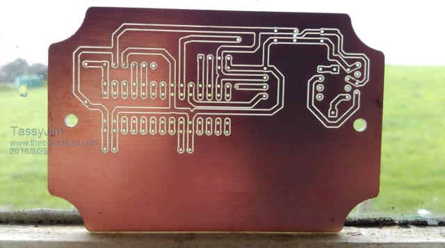
Hi Tony, Yes 3D or CNC are of more interest to me than "gerbers to China" but (to my thinking) they are not yet at the availability/price for small volume DIY?? Here is an example of a small board I recently made via Jaycar Press 'n Peel. This is the type of thing I have in mind (the layout is via Diptrace, manually routed). Veroboard is easy enough but I want to make four of them so is bordering on being a PITA. (I don't yet have the skills to take the Diptrace layout to gerbers) Cheers, Andrew  |
||||
| Warpspeed Guru Joined: 09/08/2007 Location: AustraliaPosts: 4406 |
Any CNC machine is probably going to work out a lot more expensive in the end, than some "Gerbers to China" PCB design software. And you still will never be able to do plated through holes with CNC. Going the mechanical CNC route would require a good solid high precision machine which would very likely be beyond most peoples ability to successfully home brew. It may still be worthwhile though, if you have some other totally different applications for the same machine in mind. I have very distant memories of a home built XY pen plotter. That was back in the days of DOS, 130mm floppy discs, and dot matrix printers. I eventually gave up because it was never able to create the drawing quality I really hoped for. Ended up buying a commercial Roland XY plotter that worked like magic. Still have that here somewhere. Cheers, ĀTony. |
||||
| Andrew_G Guru Joined: 18/10/2016 Location: AustraliaPosts: 840 |
Tony, Arrh yes - I used to have a beaut flat-bed xy plotter (30 years ago - stayed with the ex, along with a lot of other stuff, eg a 15" band saw). Easy to write to but probably not strong enough to mount a dremel to. Whereas if/when 3D can easily do PCBs then I'll be interested. Andrew |
||||
| Boppa Guru Joined: 08/11/2016 Location: AustraliaPosts: 814 |
I've used the special pen (and even liquid paper /liquid paper pens) as well- work surprisingly well they do- dse had (many moons ago) a triple pen pack, with various sized tipped pens from a fine tip up to a marker pen style one- dont know if anything similar is available today? re 3d printing/milling- there are metallic/conductive plastics available but not all machines can handle them and I still havent seen anyone using them much for pcb style work, milling machines on the other hand are quite common and relatively cheap, in fact I am in the process of building a small one atm especially just for pcb/front panels etc (and other small work)- one day I'd like to make a full sheet one for woodworking (ie 4x8ft) but this one is going to be just big enough for a rack panel front panel or a uncut pcb sheet eta you would be surprised at just how easy it is to do accurate 3d work these days Warpspeed, Ive built a 3d printer that had less thaan 0.2mm repeatable accuracy, and the mill when finished might be even better now I've built one, I know what not to do lol have a look at CNCzone for some of the work people are doing with homebuilt machines |
||||
TassyJim Guru Joined: 07/08/2011 Location: AustraliaPosts: 5901 |
 One of my early attempts with a CNC. Traces, holes then outline all in one sitting. It takes a bit of fiddling but once I had a procedure that works, I was happy with the results. I stick to single sided boards. Etching will get finer traces. Jim VK7JH MMedit ┬Ā MMBasic Help |
||||
| Boppa Guru Joined: 08/11/2016 Location: AustraliaPosts: 814 |
One thing I havent seen for a while, I used to use them years ago, was the 'through hole rivets' for diy doublesided pcbs... I used them with homemade etched boards- you could use the old 'solder both sides of a leg' system, but that was awkward on some components (like single ended electrolytic caps), these were a hollow 'rivet' made of copper that had one end already 'belled' into a inverted cone shape, and you did the other end either with a special tool, or like me, used a centerpunch and then a pair of multigrips... made through hole 'plating' easy as eta nice pcb btw eta2 these 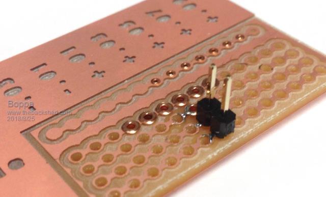 from http://fab.cba.mit.edu/classes/863.16/doc/tutorials/PCB_Rivets/ |
||||
| Warpspeed Guru Joined: 09/08/2007 Location: AustraliaPosts: 4406 |
They are still out there Boppa, on e-bay too... https://www.ebay.com/itm/500x-best-quality-pcb-copper-via-vias-through-hole-rivets-5-sizes-100pcs-each/223078735988?hash =item33f0876074:g:AbgAAMXQDHpRjAbE And the PCB etch resistant pens as well. https://www.ebay.com.au/itm/5pcs-CCL-Anti-etching-PCB-Circuit-Board-Ink-Marker-Pen-For-DIY-PCB/263718807220?hash=item3d6 6dda6b4%3Am%3AmSMBjr5ZgcX4QptnJ1Wslqw&var=562897731401 Cheers, ĀTony. |
||||
bigmik Guru Joined: 20/06/2011 Location: AustraliaPosts: 2870 |
Crikey, I only just caught this thread.. Sounds like a history of my life (sans the milling PCB era) I used to make Letra-set/Bishop tape style masters on clear overhead projector sheet and get them photo reduced to single size.. Then if single sided I made my own PCBs or double sided I sent them to a local PCB house. These places have all gone to `god' now but I used them all. Sunbury Printed Circuits Australian Printed Circuits Micro-Etch Bay-Side PCB (Or similar name) BEC (these may still be around but they changed from Australian made to China made but kept their Aus prices. I never used those little rivets, if I needed though hole on a DS PCB (I did make a few) I used wire I stripped from copper braided wire and soldered it top and bottom unless it was an axial component and could be top soldered (I used machined pin IC sockets for the ICs as they can be top soldered as well. I wouldnt consider doing them now.. The worst part was drilling the holes but I know the feeling when `IT WORKS' and I made the lot and usually on the same day. Good luck Kind Regards, Mick Mick's uMite Stuff can be found >>> HERE (Kindly hosted by Dontronics) <<< |
||||
| Tinker Guru Joined: 07/11/2007 Location: AustraliaPosts: 1904 |
Andrew, a few tips if you are set to do the home PCB etching bit. Make the 'land' of the pads as large as possible - I prefer square or rectangular pads for that reason. The ones shown in your example above at the connector would be difficult to etch or drill. For the same reason make the 'hole' in the pad small enough so it etches well but not so big that it would be hard to center your PCB drill. PCB drilling is not much fun IMO, even when I use a good pedestal drill with a comfy seat and foot operated switch plus a magnifying glass and illumination from above & below (small LED torch stuck in the center hole of the drill table) Ferric cloride etching is very messy, I used it far too long until I saw the light and changed to that granule stuff (whatsitsname?) that was dissolved in water and required heating in my etch tank. That liquid remained translucent (blue)so the etching process could be monitored through the perspex etching tank. A bubbler sped up the etching too. With the ferric cloride I had to check the progress by removing the board from the tank and letting the now black ferric cloride run off so as to make visible what was happening. I only used the toner transfer method for my single sided boards, another learning curve to get that right. The sheets for that available from the local electronic parts shop were useless - those cheap A4 ones I got on e-bay were much better, have fun. Klaus |
||||
| Warpspeed Guru Joined: 09/08/2007 Location: AustraliaPosts: 4406 |
Amonium persulphate. Cheers, ĀTony. |
||||
| Andrew_G Guru Joined: 18/10/2016 Location: AustraliaPosts: 840 |
Hi All, thank you very much. All good advice. I'm sure that when I have finished this "hairy shirt" phase (to quote Geoffg) I'll graduate to "gerbers to China" (or 3D or CNC or??). By coincidence I use ammonium persulphate so I'll stick with that. If using coated Cu and UV light what do you use to develop the exposed image, ie before etching? Do you tin the cleaned Cu prior to drilling or do you leave it as bare Cu? (If so, why?) Jim - is that view from your house? - great Klaus - is that your yacht in your avatar (I have a Van deStadt 34) is it on the Lakes? Mick - my little PCB is to piggyback your Serial Backpack Cheers, Andrew |
||||
| Page 1 of 3 |
|||||
