
|
|
Forum Index : Electronics : all home built solar system
| Author | Message | ||||
| poida Guru Joined: 02/02/2017 Location: AustraliaPosts: 1388 |
Could you tell me more details of the new battery? make and model etc? Even got some good specs? That would be useful for me. wronger than a phone book full of wrong phone numbers |
||||
| Murphy's friend Guru Joined: 04/10/2019 Location: AustraliaPosts: 583 |
Poida, These are the ones I got:batteries 4 of these packs for my 48V nom. system. Keep in mind that a good cell balancer is required for lithium batteries. EV power sells their own brand but I got the deligteen brand directly from the manufacturers, they work well and are easy to connect. 2 main reasons why I choose these batteries, they come neatly strapped already which is something I had to do with my earlier LYP individual cells. Other reason was they were local in WA and I could pick them up from their Perth warehouse and thus avoid expensive transport costs. There is more technical detail on the EV power website if you look for it. |
||||
| poida Guru Joined: 02/02/2017 Location: AustraliaPosts: 1388 |
I believe I have achieved lift off. The power board PCB design is done. I want to provide a complete home built battery based solar power system for all. All PCB files will be compatible with EasyEDA. All firmware runs on Arduino hardware and within it's IDE. All open source. 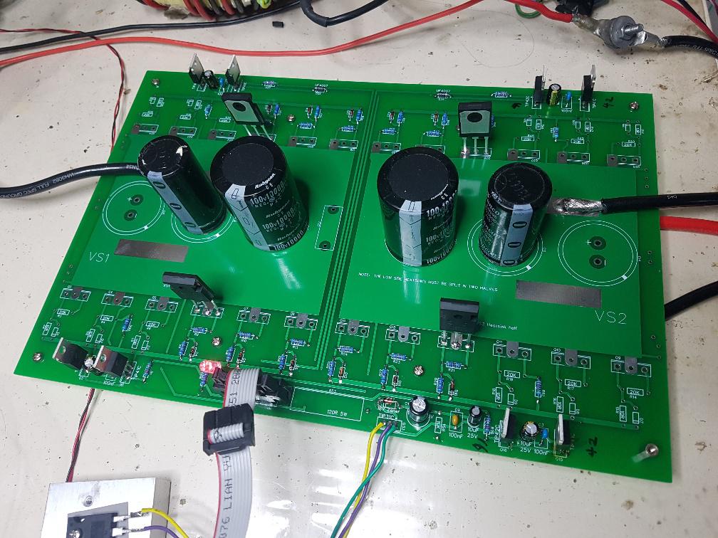 Just testing at the moment. Tomorrow I fit 3 x 4 FETS and heat sinks, the install in the victim inverter and then start the air compressor. It will either work or not. Here is the output voltage with zero load. A nice sine wave. 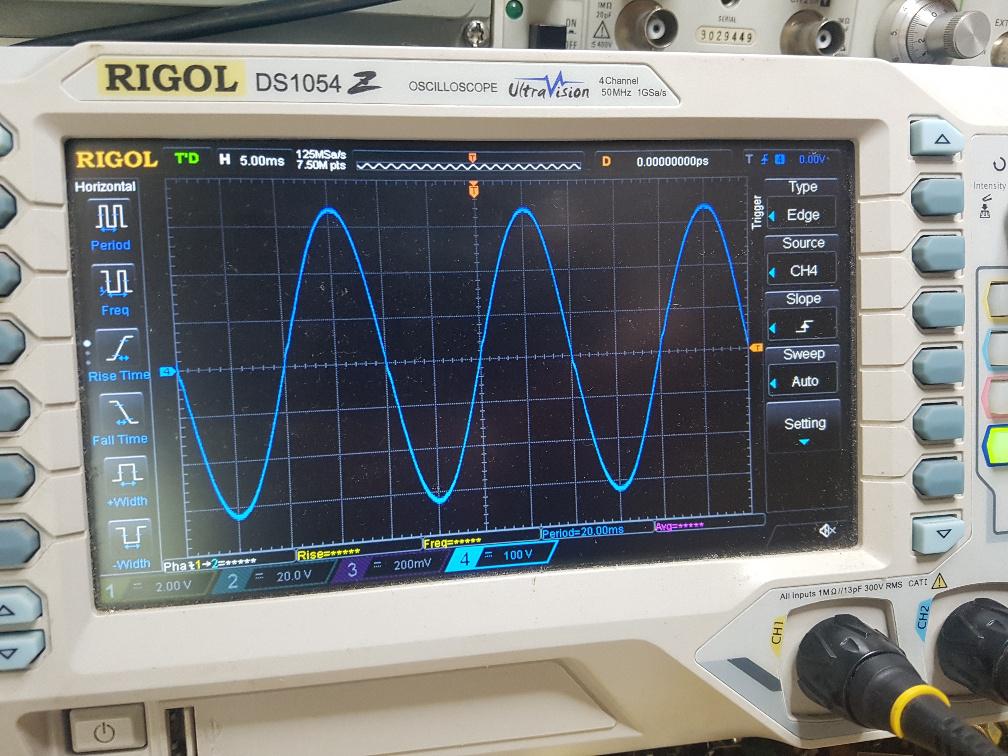 One error in the PCB tracks and 4 errors in the PCB silk screen. Not too bad for a first go at a 6kW power board. I can't complain. wronger than a phone book full of wrong phone numbers |
||||
Haxby Guru Joined: 07/07/2008 Location: AustraliaPosts: 418 |
Looks good Poida! If you are spinning another board, I'd suggest putting holes in the PCB for mounting the heatsinks. With my warp power board, I made it compatible with this pre-drilled TO247 heatsink from Ali express. The dimensions are all in the product description and it saved a lot of work. Even better when it all lined up nicely. The spacing of each MOSFET on mine is 22mm. But there are others to choose from.  |
||||
| poida Guru Joined: 02/02/2017 Location: AustraliaPosts: 1388 |
the FET spacing is 24.5mm. This is to allow those of us who have used Madness's boards to reuse the heat sinks. wronger than a phone book full of wrong phone numbers |
||||
| BenandAmber Guru Joined: 16/02/2019 Location: United StatesPosts: 961 |
Wow incredible!!! be warned i am good parrot but Dumber than a box of rocks |
||||
| Haxby Guru Joined: 07/07/2008 Location: AustraliaPosts: 418 |
Ok never mind the MOSFET spacing. Heatsink mounting holes in the PCB are always a good idea though especially if you are still in the first version of the board. If you put some conveniently spaced 3.3mm holes 10mm north of the centre of the MOSFET pads then other builders will be able to have a choice of heatsink mounting options. If you choose the 10mm dimension then it will suit a popular heatsink profile that many Chinese inverters use. 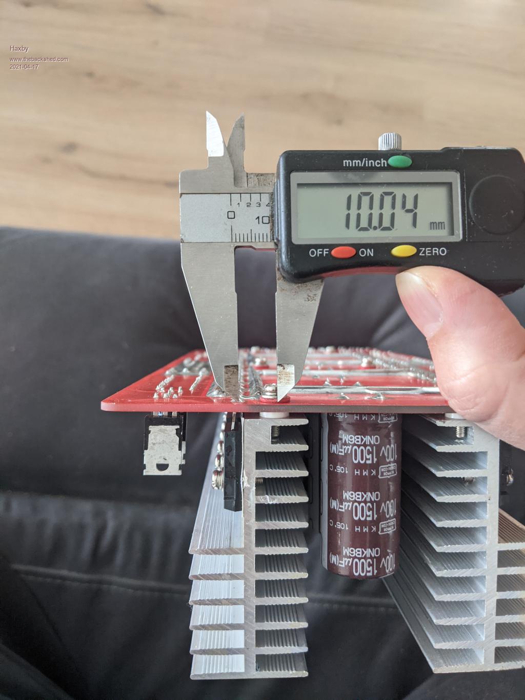 |
||||
| BenandAmber Guru Joined: 16/02/2019 Location: United StatesPosts: 961 |
I was testing some new programing on a inverter and keep blowing fets So I switched to hy5608 mosfets 360amp and instead of blowing it melts the solder and it dips off the legs I use 60/40 Kesler I like these mosfets so far They don't cost much more than the 4008 I bought them off the same guy on alliexpress that you guys recommended for the 4008 be warned i am good parrot but Dumber than a box of rocks |
||||
| poida Guru Joined: 02/02/2017 Location: AustraliaPosts: 1388 |
The power board has been tested to start the air compressor. 11kW peak power for 1/4 second. It passed easily. 3 FETS on the 4 legs of the full bridge. No RC snubbers fitted yet. (I want to see the difference they make, if any) 2 x 10,000uF 100V and 2 x 3900uF 80V caps on the DC supply rail. This is not enough but good enough for me. Errors fixed on the PCB already so we are ready to go. 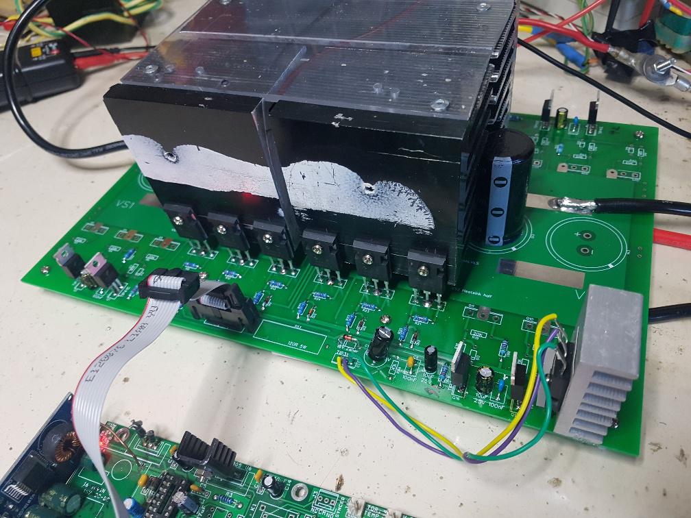 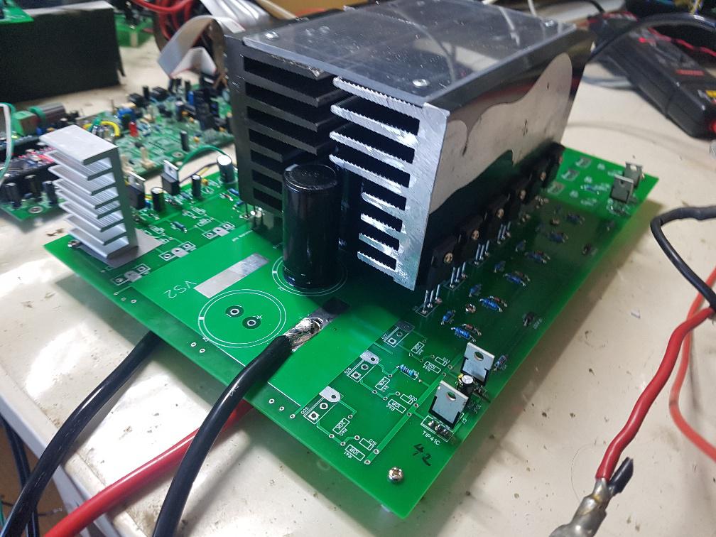 I will do further testing then post the PCB files. And basic build information for the inverter. And the code and PCB files for the nanoverter. Eventually I willpost here the complete information and files needed to do what I have done. I think it might be time to work on a simplified version of the nanoverter. It will use only one nano, and have zero communication with the outside world. We define the heatsink and toroid temperature limits for the fan and overtemp stop, a low voltage cutout and away we go. Just ground a pin to run it. I will call it the picoverter. wronger than a phone book full of wrong phone numbers |
||||
| Warpspeed Guru Joined: 09/08/2007 Location: AustraliaPosts: 4406 |
A very nice result there Peter, Well Done  Cheers, �Tony. |
||||
| Haxby Guru Joined: 07/07/2008 Location: AustraliaPosts: 418 |
Will there be any TVS diodes across the gates? Not needed? Or are they under the board? |
||||
| johnmc Senior Member Joined: 21/01/2011 Location: AustraliaPosts: 282 |
Thanks Peter for the inverter pics and apdate most impressed . cheers john johnmc |
||||
| poida Guru Joined: 02/02/2017 Location: AustraliaPosts: 1388 |
They are not needed. The totem pole driver on the power board is very good in insulating the problems of induced gate voltages getting to the IR21844 chips. It absorbs them easily and very little or zero ends up going back into the control board. I find this is the solution to the problem. (use totem pole drivers on the power board.) Very little if any voltages are sent back from the two transistor's base pins to the gate drive ICs. Even when delivering large power levels. The Aliexpress power boards that use the EG002 driver modules all (except one) have the weakness that requires protection of the gate drive IC outputs. The 3 pins of the MOSFET have capacitors connecting each other. It might not seem that is the case but in the real world of electronics parasitic effects are present. When the Drain pin sees a fast changing voltage or current, the Gate pin will see a voltage spike due to the capacitive coupling of the Gate and Drain. This voltage spike can be such that once it appears on the gate drive IC output pins, it is now well below or above the specified allowable voltage. And it blows the output drive after a while. And we clean up the broken MOSFETs then. wronger than a phone book full of wrong phone numbers |
||||
| Murphy's friend Guru Joined: 04/10/2019 Location: AustraliaPosts: 583 |
Many people on this forum seem to be copying the power board layout from the Chinese with regard to placing the big capacitors *inside* the heat sink where they get nice and hot and might have a shorter life. A simple solution is to place them on the underside of the PCB which also has the advantage of more heatsink fin area. I have long ago adopted the 'power capacitors on the other side' approach for my mosfet power boards. I also make these boards as two identical half bridges which has the advantage of smaller, cheaper boards, getting away with 1oz copper PCB's and a more flexible way of mounting the boards on both ends of the heat sink. I write this as a suggestion for anybody who likes to lay out their own PCB, not as a criticism for your work. |
||||
| nickskethisniks Guru Joined: 17/10/2017 Location: BelgiumPosts: 411 |
You can call it Chinese, but it's a technique Mastervolt,Victron and Studer used in their (some older) designs, just to mention some brands. In my opinion there's is nothing wrong with that if you know the pitfalls like you said. You say temperature could cause issues, yes, capacitors are degrading faster with higher temperatures. But with poida's software you can easily adjust the parameters to start the ventilation as soon as you want and due to the heatsinks the wind is guided perfectly around the capacitors. Only 1 fan is needed to cool down the components. I agree with you that mounting the fets under the PCB could have more advantages. The cooling down of the fets could be made more efficient and even passive to achieve lower temperatures or pushing the fets harder. But I find it's a challenge to design the mechanics arround. It's on my list to draw an inverter PCB with fets under the PCB. In fact I do design my PCB's with fets 99% like that. Including 3ph and half bridge pcb's, but still not 100% satisfied about the results, I keep adding adjustments and keep thinking it's not good enough. Today I was looking at a 3ph design and I was telling to myself, why didn't I draw the +- and AC connections the other way around that would have been more logical.... One's satisfied I will post it, I plan my next build next year, I really need a spare inverter for when things go wrong. I need to look up your builds for inspiration. Btw, I know solarMike, Wiseguy and mackoffgrid to mention some forum members, have posted designs with mosfets mounted under the pcb. Edited 2021-04-19 07:22 by nickskethisniks |
||||
| Haxby Guru Joined: 07/07/2008 Location: AustraliaPosts: 418 |
So the control electronics are safe behind the totem pole driver, but what about the MOSFET itself? The gate will have a max voltage specification around 25v which may be exceeded. Or are they sturdy enough to handle it? |
||||
| poida Guru Joined: 02/02/2017 Location: AustraliaPosts: 1388 |
Haxby, my view is the internally generated voltage transients caused by the fast voltage and/or fast current changes between Drain and Source are not going to be a problem for the MOSFETs. Even if these voltage transients were a problem for the FETS, what can we do about them? Reduce the switching speeds via larger gate series resistance? That would work to some degree or other. The specifications for IR21844 and IR2110 and probably many other IR parts have the gate drive outputs to remain within -0.3V of Vss (ground) and +0.3V of Vdd (dc supply, usually 12 or 15V). This is not unreasonable since the gate drive output stage within the IC is a pair of MOSFETS and undoubtedly they are microscopic, not robust and easy to damage. I have measured voltages that easily exceed the low limit by a volt. This was when I drive a power board's FETS directly by a pair of IR21844 chips. IF the internally generated transients, when added to the gate drive voltage now exceeds the MOSFET specs then there will be trouble, eventually. I have measured gate voltages carefully on the totem pole power boards and the difference is profound. I made a post on this subject I think it's here https://www.thebackshed.com/forum/ViewTopic.php?PID=131988#131988#131988 here is a look at non-totem pole power board gate voltages https://www.thebackshed.com/forum/ViewTopic.php?PID=131506#131506#131506 Back then I was wondering about potential damage to gate drive IC output stages. wronger than a phone book full of wrong phone numbers |
||||
| Warpspeed Guru Joined: 09/08/2007 Location: AustraliaPosts: 4406 |
There have historically been quite a few issues with excessive gate voltages, but things have slowly changed over the years, where its now no longer the problem it once was. Back in the early mosfet days, mosfet gates were commonly rated for +/-20v max, but it was found that 15v of drive could lead to long term unreliability, and 12v drive was considered optimum for best reliability. Mosfet technology and quality control have come a very long way over the last few decades. You will commonly see a 10K or 4K7 resistor connected gate to source. The purpose of that is if the gate is run open circuit, and you suddenly switch say +400 volts onto the drain at power up, the gate drain capacitance will couple enough energy into the gate circuit to often blow the gate oxide layer before the mosfet can turn on to protect itself. Normally this would never happen with a gate driver chip connected, but its always been good practice to fit a resistor to high voltage circuits. Some of the switch mode controller chips use bipolar transistors, as the internal op amps and comparators are bipolar, and so is the bipolar gate driver output stage. The application notes warn that a big heavy duty Shottky diode MUST be connected between gate and source to prevent any negative spikes from latching the substrate of the driver chip. Many if not most gate driver chips these days have no analog circuitry inside, and are totally CMOS. The inherent source drain reverse diodes in the driver output stage mosfets totally protect both the driver chip and the mosfet gate from any excessive voltage transients. So its no longer common practice to fit Shottky diodes or resistors (or transorbs) into mosfet gate circuits. Sometimes you still see them, but they really do nothing useful. Peter is quite right, Mad's totem pole has solved a lot of issues. Cheers, �Tony. |
||||
| Haxby Guru Joined: 07/07/2008 Location: AustraliaPosts: 418 |
Is there a schematic of Mad's totem pole circuit? I can't seem to find it  |
||||
| poida Guru Joined: 02/02/2017 Location: AustraliaPosts: 1388 |
here is the one I used for the above power board. Schematic_powerboard_2021-04-19.pdf the 10 pin IDE socket connects to the nanoverter. It's schematic is nanoverter_D-schematic.pdf wronger than a phone book full of wrong phone numbers |
||||
