
|
|
Forum Index : Electronics : all home built solar system
| Author | Message | ||||
Haxby Guru Joined: 07/07/2008 Location: AustraliaPosts: 419 |
Thanks Poida that's cleared it up. Do you think there is any merit in adding totem poles to my HV inverter? I was having a lot of these switching problems which I solved with adding significant gate capacitance (around 82nf). The switching speed is obviously slower in a step inverter, so you can get away with more, but I feel like the totem pole solution would be better. |
||||
| poida Guru Joined: 02/02/2017 Location: AustraliaPosts: 1391 |
I don't know for sure. If you want clean and EMI tolerant gate drive I like totem pole drive, located close to the MOSFETS. I would seriously consider the TLP350 and other opto coupled driver ICs such as the FOD3182 These seem to be fast enough and can drive a couple of Amps. What is best is there is zero crosstalk from the input pins to and from the output drive pins. You can physically locate the IC within 10mm of the FETS so the lead lengths can be short as can be. You will need a small isolated 15V supply for each high side and one for the two low sides of the bridge. The TLP350 and Fod3182 specs show a totem pole output stage so you are getting that, just not from discrete components. The Recom RE1215S dc/dc converters are cheap and easy to use. Cost about $12 each. Saves me a heap of time and farting about with Aliexpress cheapies. wronger than a phone book full of wrong phone numbers |
||||
| poida Guru Joined: 02/02/2017 Location: AustraliaPosts: 1391 |
picoverter so far: 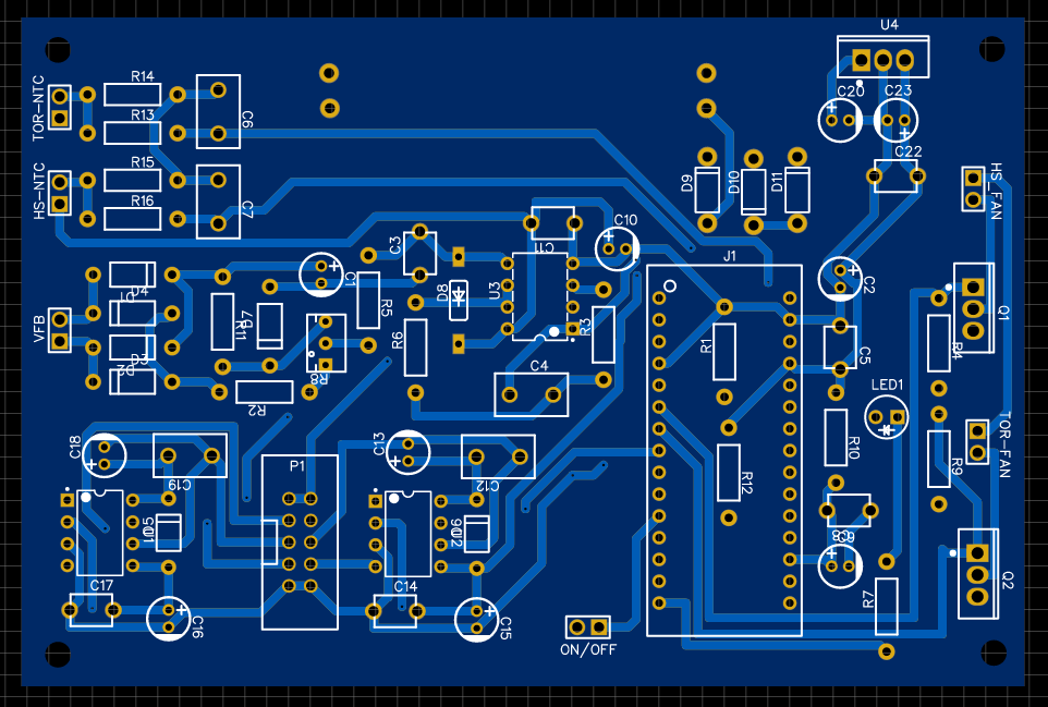 I intend to stand the dc-dc converter on it's edge and hold it in place with 4 solid copper wires. Strong as need be. The board is only 75mm x 115mm approx.  here is the schematic The dc-dc converter takes the 48V battery (46 - 56V) and makes 15V at about 1 Amp. 1 amp is needed when both fans are running. I use 3 diodes in series to drop the 15V to about 12V sort of ish and that is good enough for the fans. Saves using a 7812 regulator and more caps. This is based heavily on TinyT's work on the nanoverter. Schematic_picoverter_2021-04-20(1).pdf This controller will be perfect for workbench testing. Probably use it in the spare inverter builds in the future. wronger than a phone book full of wrong phone numbers |
||||
| nickskethisniks Guru Joined: 17/10/2017 Location: BelgiumPosts: 420 |
Hi Peter, good work! Just 2 remarks. Try to draw all horizontal lines with 1 color and do the vertical in the other color (top or bottom) that way you will always be able to cross your traces. I only started recently with that, important when things get bigger and messier... It's always good to avoid 90degree corners, I thought it was difficult to do sharp corners for the manufacturer. |
||||
| Murphy's friend Guru Joined: 04/10/2019 Location: AustraliaPosts: 592 |
And another tip for PCB layout for the home designer. Try to make the component pads as big as possible, I find those in the PCB program libraries useless for home soldering - unnecessarily small. Make the pads for connectors rectangular (with rounded corners perhaps), you get maximum surface are which will be appreciated if that part ever has to be unsoldered. Ditto for IC sockets. I usually make component pads (resistors, etc,) square for the same maximum surface reason. Double check all component pin diameters so they fit easily through the pad hole but also are not too loose so the component falls out when you turn the board over to solder the legs. The manufacturer will make track corners anyway you like, I see nothing wrong with 90 degrees. But the track separation in the above PCB is unnecessarily close, IMO, at some parallel tracks. |
||||
| poida Guru Joined: 02/02/2017 Location: AustraliaPosts: 1391 |
It's different for me. EasyEDA and JCLPCB produce boards I find easy to solder and rework so I'm fine with the library parts. This PCB was the result of spare time at work today. I chose to do it with 1mm track widths to make it hard to layout, as an exercise. No tracks went between 0.1" pins of the Nano or ICs. Probably only need 0.5mm track widths or less. It's not a big deal to rework the PCB. Something to do at work... Thanks for your advice tho. wronger than a phone book full of wrong phone numbers |
||||
| wiseguy Guru Joined: 21/06/2018 Location: AustraliaPosts: 1003 |
Peter, I can see the progress you are making with the PCB design, its certainly faster than my software progress...... A couple of small critiques that jumped out at me, C2 & C10 have the two + & - tracks too close, they should have more clearance. Maybe they would benefit from a 90 degree clockwise rotation, but this is without the benefit of seeing underneath - maybe there was a constraint. The negative track on C15 & 19 also bends too close to the + terminal, just extend from the capacitor before the 45 degree bend. Lastly a few tracks seem very close to other tracks and I am not convinced they need to be that close. Reasonable clearances for manufacture should be maintained etching pcbs is not a perfect art and you can assist to get a better result without microscopic shorts. If at first you dont succeed, I suggest you avoid sky diving.... Cheers Mike |
||||
| Warpspeed Guru Joined: 09/08/2007 Location: AustraliaPosts: 4406 |
When you go to the PCB manufacturers quotation page, and select the various options, among them are minimum track widths and clearances. What you might consider very very small are to them absolutely enormous. Long gone are the days of etching your own boards in the kitchen sink. And professional boards never come back with microscopic shorts or open tracks. These days every track, and every via, on every board is probed and 100% tested by a robot that has the complete net list to work from. Cheers, �Tony. |
||||
| wiseguy Guru Joined: 21/06/2018 Location: AustraliaPosts: 1003 |
I had some RM6 transformer windings made with tracks of 6mil width and 6mil spacings. Some came back with shorted turns on windings - it sure as hell had 100% tested continuity - even including some unintended short cuts. It took a microscope and sharp scalpel to find and fix. If there is a good reason for tight spacing I'm all for it and do it. If there is ample space there is no need to use tight spacing. In my experience when so close to a solder joint too, it is just asking for trouble. If at first you dont succeed, I suggest you avoid sky diving.... Cheers Mike |
||||
| wiseguy Guru Joined: 21/06/2018 Location: AustraliaPosts: 1003 |
It appears robots may still have a bit more to go to achieve perfection yet, and I wont be letting one drive me around any time soon. Edited 2021-04-21 20:02 by wiseguy If at first you dont succeed, I suggest you avoid sky diving.... Cheers Mike |
||||
| poida Guru Joined: 02/02/2017 Location: AustraliaPosts: 1391 |
Thanks everyone for your thoughts on the PCB. I will take notice of all you have written. It is clear I need to rework it with some care for good clearances of tracks. Working current levels are only about 100mA so I do not need 1mm wide tracks as well. A bit of care might bring the ground, 5V and VBAT (50V) tracks down to a smaller length but retain 1mm width. All the signal and decoupling lines could be 0.25mm or something. When laying out the above board, I found it easy to first route small parts of the board in a location well separated from the PCB then move the completed section into place on the PCB. This makes the large job a collection of easier to tackle smaller tasks. Tomorrow is day 2 of my working week. I work 4 days, 2 at work, 2 at home. PCB routing is a job for a day at work. wronger than a phone book full of wrong phone numbers |
||||
| wiseguy Guru Joined: 21/06/2018 Location: AustraliaPosts: 1003 |
Warp once again you have posted something I consider derogatory to a post I have made and it has annoyed me enough I feel the need to take you to task over it. If I (or others) post something that is just plain wrong or totally misleading by all means post your own experience or opinion, but be careful & respectful of others points of view which may differ from yours - it does not make you right or others wrong that they have had different experiences. I can think of many instances in my designs where just because something has the same net doesn't mean I want them connected together wherever the PCB fabricator feels like joining them with crappy etching and inspection. I run sometimes long traces for instance where a kelvin connection is routed back to circuitry for precision or noise free measurement - yes the same net as the ground plane with its multiple instances of connections surrounded by a ground plane and very narrow annular & linear clearance but there is no way I want them joined anywhere except where I specifically join them. Ultra high speed memory can have multiple buses that are critical to have the same track length, this involves purposely weaving a track back and forth at times to use up length with minimum clearances involved, again the same net but a bad etch can undo your hard work and cause issues that are hard to find or fix. I was even really clever on a big project and placed hard wired addresses on a back plane with multiple charging units that plug in, all with serial comms, This was done by selectively having plated through holes in a dual grid of pads for address line selection, but I even put annular pads with a centre void but no hole in case I ever wanted to drill through to a like pad underneath and change an address/bank addressing. The PCB fabricator was so helpful he drilled and plated through all these holes for me where he assumed they were meant to be without consultation ! There are also PCB track antennas & loops with stub connections, pcb baluns that might have the same net but they dont share the same function, planar coil windings etc. I simply posted that unless it is necessary to have tight clearances it is not best practice to rely on the fabricator to get right what you perhaps could have avoided with a little extra care. I was not trying to big note myself or criticise Peters creation, I still consider my advice as valid despite your negative response overtones & claims that PCB fabricators dont make mistakes or pick them up before delivery - that would be a false assumption in my experience. My RM6 track windings were 6/6 mil, their capability is supposedly 5/5 mil for general 1oz boards and I have found more than 1 issue with the 10 returned arrays of boards. If at first you dont succeed, I suggest you avoid sky diving.... Cheers Mike |
||||
| nickskethisniks Guru Joined: 17/10/2017 Location: BelgiumPosts: 420 |
I don't want to pollute Peter his thread but Wiseguy, I think Warpspeed is here for helping too. But I agree with you about your statement about "professional" pcb manufactures. At work we had (have) issues too, I'm not part of the designer team but sometime I do test populated pcb's and do the problem solving. And it happens that tracks are shorted to each other, after talking to the designers lots has to do with the way the pcb was designed, for instance it's not good to have a lot off "open space" where there are no tracks or no copper plane. When there is lots of open space the copper tents to build up around the tracks during manufacturing and you can have shorts between the tracks. Could be the manufacturer has some issues at their quality control stage, but we only work with (reliable?) European manufacturers, prices are like 10x compared to easyeda, 60eur for a 2 layer Eurocard format is no exception. Of course it's possible some Chinese companies have better machines.  |
||||
| Warpspeed Guru Joined: 09/08/2007 Location: AustraliaPosts: 4406 |
Perhaps I have just been extremely lucky, but in all the years I have been having boards made for me by reputable companies, I have never once received a board back that was faulty due to a manufacturing stuff up. But I can certainly see your point. Something like a very fine spiral track COULD have a copper bridge and a shorted turn, and it would not show up during automatic testing for continuity. It SHOULD have failed visual inspection before the solder mask was applied. It may also be difficult to convince the board manufacturer that it is in fact faulty, unless a short is plainly visible. Don't really know the answer to that one. But I can only go on my own personal experience, which seems to be rather different to your own. Cheers, �Tony. |
||||
| Murphy's friend Guru Joined: 04/10/2019 Location: AustraliaPosts: 592 |
Poida, I found a youtube that might interest you since earlier you mentioned lithium batteries for your bank. This describes how adding lithium batteries to your LA bank might benefit both. lithium + LA marriage |
||||
| Warpspeed Guru Joined: 09/08/2007 Location: AustraliaPosts: 4406 |
That is brilliant Klaus !! Cheers, �Tony. |
||||
renewableMark Guru Joined: 09/12/2017 Location: AustraliaPosts: 1678 |
The point he is making at 6 min mark is VERY important for us that are off grid and rely on winter cloud to provide all our needs. So basically if this were to be done in my setup that is already configured for flooded LA how would you hook up the lithium to a charger? Would you just let the existing charger take care of it and the cell balancer on the lithiums will look after them individually? It's a very good point he is making combining the two, I'm just a bit concerned about charging. Cheers Caveman Mark Off grid eastern Melb |
||||
| renewableMark Guru Joined: 09/12/2017 Location: AustraliaPosts: 1678 |
Currently my system gets a 57.6v absorb charge for 2 hours each day then goes to float at 54v, would that charge profile suit lithium? Lowest voltage I normally see is 50v by morning in winter. It's amazing what the fan in the central heating takes to run from sundown to sun up. Cheers Caveman Mark Off grid eastern Melb |
||||
| Solar Mike Guru Joined: 08/02/2015 Location: New ZealandPosts: 1128 |
Flooded LA. has to have a periodic higher voltage profile in order to stir up the electrolyte to prevent stratification; your 57.6 is going to be too high for long term Lifepo4 charge. 54v float is also little high unfortunately. I think he may have been talking about sealed LA, batteries, for a boat anyway, for this application. The video recommends max (12v system) of 14V or 56v (48v bank) which is ideal for Lifep04 at 3.5 V\cell, the difference in capacity to bring them up to max at 3.6v is only a few amp hours (400 Ah bank). I run my lithium's at 3.475 V\cell max during the balance phase and may only last 30 min, before dropping to approx 3.35 V\cell for float, at this setting bank capacity drops down approx 10 AH and sits there with zero charge current if there is no load on the system. When loads occur the PV charger supplies all of it if there is enough sun. Very interesting video though, and worth doing if you have sealed LA batteries. Cheers Mike |
||||
| Murphy's friend Guru Joined: 04/10/2019 Location: AustraliaPosts: 592 |
Agreed that this idea is meant for sealed AGM batteries, which is the type poida shows in his picture and the post was meant for his set up. One thing about those 12V lithiums the video mentions, which have a BMS built in. I use these in my caravan, 2 x 12v/120Ah in series for a 24V system. Now, there is a great variety of those 12V lithium batteries on the market and some I saw advertised on ebay have a rather poor performance. I would suggest choosing one that can handle up to 100A charge/discharge, some of the ones I saw have less than half of that and are, consequently, cheaper. For a home battery bank you want some decent instant current discharge capability and also the battery can accept a decent charging current. At least all the current the charging method (and future expansions of it)can throw at the battery bank. I have seen 90A flowing into my home 300Ah/48V battery bank and they just gobble it up. Momentary discharge currents would be higher than that if I start up some machinery. |
||||
