
|
|
Forum Index : Microcontroller and PC projects : LCD + Pico combo
| Author | Message | ||||
| Zonker Guru Joined: 18/08/2012 Location: United StatesPosts: 767 |
Good afternoon Gents.. Just saw this thread a few days back and a fresh Pico with V5.07.00a47 seems to be working on a vector board.. I am a bit late to this thread but would love to have a copy of that awesome PCB when available... For now I want to try hooking up the circuit and see if I can get the ILI9341 Display and SD card to work.. I was looking in another thread to see what the INIT code would be for it... Will try and get it going... Much thanks for all the work done with this awesome $10 board... Even has a 12 bit ADC... Nice... |
||||
| vegipete Guru Joined: 29/01/2013 Location: CanadaPosts: 1127 |
V1.03: changes: Capacitors C1 and C2 relabeled, Speaker redrawn as 12mm R4 shifted for more space J7 labeled Vreg reversed left/right Pad/drill sizes juggled here and there slightly. Can you confirm the Pico pin spacing is .700 inch? Also, where is J7 likely to be connected to? Easy to run traces now... 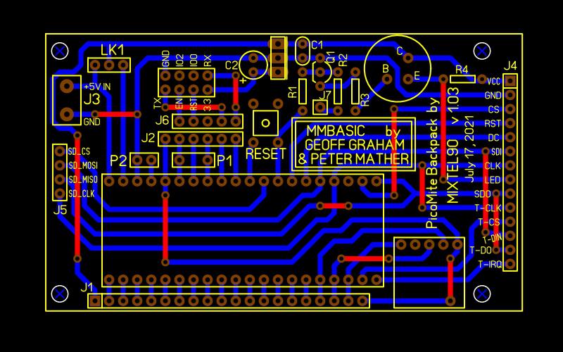 Visit Vegipete's *Mite Library for cool programs. |
||||
| Mixtel90 Guru Joined: 05/10/2019 Location: United KingdomPosts: 7815 |
The official drawing for the Pico gives 17.78mm. By some curious coincidence that works out at bang on 0.7". :) I left J7 disconnected as it may not be needed at all and would only be using a pin unnecessarily. Additionally, I'd used all the IO pins on that side of the Pico and single-sided routing from the other side would have been a pain. For non-square waves it would go to a PWM pin. I *think* it would be on any free IO pin for GUI BEEP but I've never used that. If someone wanted to they could connect an off-board 5V relay with parallel diode to the drain of Q1 and +5 and get a clean contact out instead of using it for sound. :) I think leaving it free gives maximum flexibility. If you consider it a good idea to put a pin close to J7 (a 2-pin link might be a good idea) then I think I'd suggest GP11 (PWM5B). It's in a logical position on the circuit diagram and is probably one of the easiest to route on the PCB. Pin spacing on C1 could be 0.1" or 0.2", but it's not something I generally worry about. It's easier to jam a 0.2" cap into a 0.1" pcb than the other way round. :) Edited 2021-07-18 04:03 by Mixtel90 Mick Zilog Inside! nascom.info for Nascom & Gemini Preliminary MMBasic docs & my PCB designs |
||||
| lizby Guru Joined: 17/05/2016 Location: United StatesPosts: 3347 |
Might it not be well to add 3V3 and 0V to J5, the ILI9341 SC connectors, so that a separate SD card module could be added if one used an ILI9488 or an ILI9341 which was of a different size? PicoMite, Armmite F4, SensorKits, MMBasic Hardware, Games, etc. on fruitoftheshed |
||||
| vegipete Guru Joined: 29/01/2013 Location: CanadaPosts: 1127 |
V1.04: J7 can be jumpered to GP26 - PWM5A, More labelling, Extra pads around J3 so that a CJMCU USB jack fits. 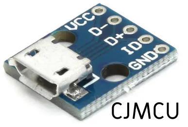 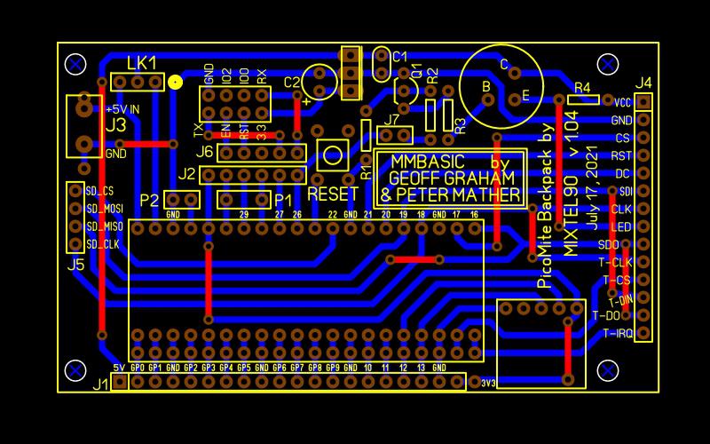 Visit Vegipete's *Mite Library for cool programs. |
||||
| Mixtel90 Guru Joined: 05/10/2019 Location: United KingdomPosts: 7815 |
That's fine. The mosfet could be wire jumpered to somewhere else if the ADCs are wanted. I've not used the CJMCU before. Neat option if it will fit. :) Why the extra row of pads for the Pico and adding an extra blank pad on J1 next to 3V3? @lizby We might be able to put a pair of unequipped pads, but J5 can't be extended to either side. SDCLK is almost hard up against the USB plug on the Pico. The pads could have a 90 degree connector on the copper side, between this pcb and the display. Edited 2021-07-18 06:36 by Mixtel90 Mick Zilog Inside! nascom.info for Nascom & Gemini Preliminary MMBasic docs & my PCB designs |
||||
| Volhout Guru Joined: 05/03/2018 Location: NetherlandsPosts: 5021 |
I havent checked in detail, but currently the pico has pins 1-15 to the external header. And a second header has adc pins. Could it be possible to use the other spi bus for system, rotate the pico, relocate the other pins, so we can connect pi pins 21-40 directly to the 20 pin header. In essence, move all circuits on the backpack board to pi pins 1-20. Volhout PicomiteVGA PETSCII ROBOTS |
||||
| vegipete Guru Joined: 29/01/2013 Location: CanadaPosts: 1127 |
Any time I've been hacking boards for miscellaneous projects, extra holes/pads have always been welcome. I managed a second row of Pico paralleling pads on the other side too - they may never be used, but if even one person finds a use, they're worth it. I'll try to add even more 5V, 3V3 and GND pads if possible. Another valuable feature is the 2 ground jumper pads near J3. A loop of wire there provides a place to clip 'scope or analyzer ground leads. I left the last pin of J1 un-labeled because it is a power pin right beside Pico data pins and mis-reading/understanding the labeling seems quite possible and could fry pins. Visit Vegipete's *Mite Library for cool programs. |
||||
| vegipete Guru Joined: 29/01/2013 Location: CanadaPosts: 1127 |
Maybe to fit something like this: micro SD module Visit Vegipete's *Mite Library for cool programs. |
||||
| Mixtel90 Guru Joined: 05/10/2019 Location: United KingdomPosts: 7815 |
@Volhout I considered putting all the IO together but made a conscious decision not to because they are analogue pins. As it is a simple daughter board can be plugged into J2 to simultaneously add a voltage ref and, say, a couple of 0-10v inputs. AGND is there too, to keep noise down. There are PWM, UART, SPI and I2C all available on J1. I brought out as much as I could. Remember - this was originally designed to be a simple PCB too, that could be made DIY. @Pete I think that if you are going for safety on J1 then the pin to isolate/move is the 5V output. No inputs on the Pico can take that but the 3V3 is ok, even if it's next to a GND as the SMPS will shut down on overcurrent if they are shorted. The extra pin makes it a 21 pin connector too. :( Just an idea... Nudge the 5V pin out by 0.05" so that if a 20-pin connector is used it can't be connected. TBH, useful though it may be to some I find it scary. lol 3 pads for 5V, 3V and GND for a copper-side 90 degree connector under the Pico might put everything there for 5V to external stuff and a different SD card. I thought the extra GND near J3 was to connect the CJMCU. Edited 2021-07-18 07:36 by Mixtel90 Mick Zilog Inside! nascom.info for Nascom & Gemini Preliminary MMBasic docs & my PCB designs |
||||
| lizby Guru Joined: 17/05/2016 Location: United StatesPosts: 3347 |
Right. That's what I use, but the pinout doesn't align with the SD pinout of the LCD SD pins. But 3V3 and 0V somewhere nearby would help (but don't want to over-complicate). PicoMite, Armmite F4, SensorKits, MMBasic Hardware, Games, etc. on fruitoftheshed |
||||
| vegipete Guru Joined: 29/01/2013 Location: CanadaPosts: 1127 |
V1.05: J3 pushed around to top edge to make room for alternate uSD card, as linked previously, (CJMCU USB jack goes underneath now) Voltage on J1-1 selectable with LK2 (near clock module), Most traces reduced to 24 mil width, except for main power traces. Board could still be fabbed as single sided with jumper wires, except for "ALT uSD", Both sides of Pico have spare row of pads for custom butchering, er, customizing, Pins IO0 and IO2 of ESP8266 access pads added, in case someone needs 'em, Silly graphic added to real-time clock footprint ;-) 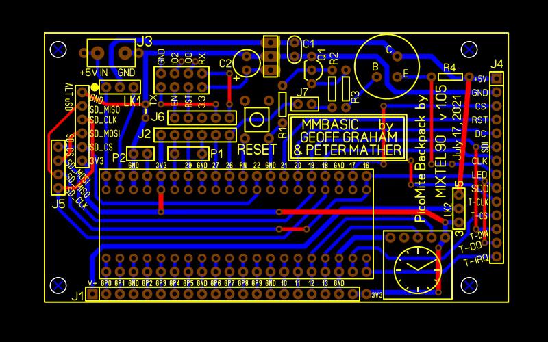 Visit Vegipete's *Mite Library for cool programs. |
||||
| lizby Guru Joined: 17/05/2016 Location: United StatesPosts: 3347 |
Sweet. What CAD software? PicoMite, Armmite F4, SensorKits, MMBasic Hardware, Games, etc. on fruitoftheshed |
||||
| Mixtel90 Guru Joined: 05/10/2019 Location: United KingdomPosts: 7815 |
I know it's a late stage, but I've been re-reading the Pico docs. The primary power into the system should be on VSYS, not VBUS. This is bacause VBUS feeds VSYS via an on-board schottky diode to protect the PC USB from an externally powered PICO. Consequently I suggest that we dispose of LK1. J3 in would feed VSYS via a 1A schottky diode (to prevent VSYS back-feeding into J3), VBUS would be connected to a pad only. This gives the "simple" alternative supply in the Pico datasheet. However, by removing the diode VBUS, VSYS and J3 are all available for re-connection using a P-FET and/or battery charger as described in the same document. That's the easy way. The hard way is to fit the P-FET, but I doubt if there's any point really. The Pico isn't all that fussy about it's 5V supply. By removing the diode and linking the VBUS pad to J3 the Pico is correctly powered for using the USB port in host mode. supply_detail.pdf (I'm frantically keeping up with the circuit mods as we go along. :) ) I know there's a lot of links etc. on this board, but I don't want to fall into the trap of the original backpack, where so many options are hard-wired to IO that you need to make serious pcb and software mods to get an analogue or PWM. Even now, without J7 you would lose all the ADC pins if you wanted to use the speaker (you can't use ADC 1 and 2 without allocating ADC0). Incidentally - if anyone wants to try to put all IO on a single connector - I'm pretty sure that you can't do it on this size of board without running tracks between Pico pins. I tried. Also, the pico is slightly longer than the height of the board. :) If I'd wanted to use a different display then that would have been ok, but I'm aiming for a minimum cost basic system. Edited 2021-07-18 18:26 by Mixtel90 Mick Zilog Inside! nascom.info for Nascom & Gemini Preliminary MMBasic docs & my PCB designs |
||||
| vegipete Guru Joined: 29/01/2013 Location: CanadaPosts: 1127 |
I'm drawing this with Sprint Layout. Note about board size: As drawn, the board is 50x86mm, which exactly matches the ILI9341 module on my desk. Stretching the board to 100mm wide with a 'sea of holes' (or maybe just a 'small pond of holes') would still allow 2 boards per 100x100mm cheap PCB offer from various board houses. V1.06: I think I understand the change requests: LNK1 is gone, D1 sort of in its place, J7 moved to GP28, which is AN2, I think, A bunch of extra pads beside D1, some 5V, some GND, one 3V3, plus 3 isolated. 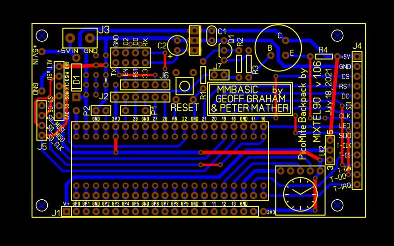 Visit Vegipete's *Mite Library for cool programs. |
||||
| Volhout Guru Joined: 05/03/2018 Location: NetherlandsPosts: 5021 |
Swap C an E at the backlight transistor footprint . PicomiteVGA PETSCII ROBOTS |
||||
| Mixtel90 Guru Joined: 05/10/2019 Location: United KingdomPosts: 7815 |
Yep, that looks right. I didn't think there was space to get a track from J7 to GP28. Neat job! :) LK2 could be LK1 now. On this particular build I'm not in favour of going outside the dimensions of the display. My concept for it is as a module to be used in other equipment, not as a development platform so, unless the holes area could be easily snapped off, then I don't like the idea. As it is the module will fit into a small, standard plastic box if the ESP is left off and a slot cut for the SD card. I originally tried to get the ESP within the display area too, but decided that the antenna was probably better if further from the board and that if the module was put in a metal box then it would be useless anyway. It was low on the list of priorities - more of a "nice to have space for". Having said all that, I've started looking at the idea of an intelligent IO extension that goes between the display and this pcb, using long pin headers for "pass through" display connections and picking up on the RTC I2C, GND & 3V3 pins at the RH end of J1 (probably using a lead). It would hold a 28-pin MX170 connected via I2C. (Not sure what else yet). A similar idea could use a full-size "sea of holes" should someone want one. How do you like Sprint? I've done a little design on both KiCAD and Eagle. Both are good in their own ways. I find Eagle much more user-friendly but KiCAD much more professional. Edit: Quite right, Volhout. Blast these olde-worlde PNP thingies... (Q2) Edited 2021-07-19 17:01 by Mixtel90 Mick Zilog Inside! nascom.info for Nascom & Gemini Preliminary MMBasic docs & my PCB designs |
||||
| lizby Guru Joined: 17/05/2016 Location: United StatesPosts: 3347 |
Never seen the phrase "user-friendly" associated with EagleCad. It's gotten better over the years, but remains, to my mind, very "un-Windows-like". But it's the devil I know. PicoMite, Armmite F4, SensorKits, MMBasic Hardware, Games, etc. on fruitoftheshed |
||||
| Mixtel90 Guru Joined: 05/10/2019 Location: United KingdomPosts: 7815 |
It's sort of "user friendly" if you compare it to KiCAD IMHO. :) Mick Zilog Inside! nascom.info for Nascom & Gemini Preliminary MMBasic docs & my PCB designs |
||||
| vegipete Guru Joined: 29/01/2013 Location: CanadaPosts: 1127 |
For simple-ish, draw a pcb quickly, Sprint Layout is hard to beat. It has a few very minor quirks, but it is a nicely behaved Windows program and very much GUI point, drag and click. I've been using it for ages, since version 4, and have produced many boards over the years, professionally and hobby. I've dabbled with Eagle in the past - sort of got somewhere with it, but can't imagine why I would bother learn it in detail now given KiCAD's abilities. I use KiCAD for schematic capture, and slowly learn more for using it for pcb layout. 'Slowly', because Sprint Layout is so much easier, and does what I need. =========== V1.07: LNK2 renamed to LNK1, E & C reversed Bit more trace clearance from J7 to GP28 Fixed trace to T-CLK (got disconnected) Gerber and Drill Files 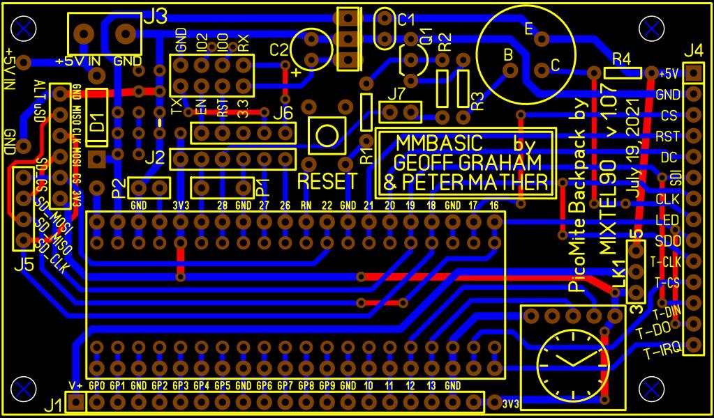 Visit Vegipete's *Mite Library for cool programs. |
||||
| The Back Shed's forum code is written, and hosted, in Australia. | © JAQ Software 2025 |
