
|
|
Forum Index : Microcontroller and PC projects : LCD + Pico combo
| Author | Message | ||||
| Mixtel90 Guru Joined: 05/10/2019 Location: United KingdomPosts: 5735 |
Would R4 fit vertically so that the link down to LK1 could also be vertical? Just a thought. You seem to have a superfluous pad on the CLK line just beneath the E in MIXTEL. I trust there's no extra charge for it? ;) ============ I like KICAD, but I found it to be like using a sledgehammer to crack a nut - and I have to re-learn it every time I come to use it. I very rarely design a PCB. I gave up on creating custom components - if I can't find something in an existing library then I don't use it. I found Eagle much easier, but of course it's more restrictive. So far the restrictions haven't been much of a problem. It's a pity nanoCAD can't produce PCB files. I'm pretty much used to that method of working after using AutoCAD and AutoCAD LT for over 30 years. lol Mick Zilog Inside! nascom.info for Nascom & Gemini Preliminary MMBasic docs & my PCB designs |
||||
vegipete Guru Joined: 29/01/2013 Location: CanadaPosts: 1082 |
Drawn as a 2 sided pcb, so the 'wire' links aren't really real.  That extra pad is actually on the LED trace. Why? It turns out some of the ILI9341 boards have the backlight drive transistor on board and only require a digital signal to turn the backlight on (or PWM it.) An extra pad seemed useful, all for an extra cost of ... nothing. Visit Vegipete's *Mite Library for cool programs. |
||||
| Mixtel90 Guru Joined: 05/10/2019 Location: United KingdomPosts: 5735 |
Erm... yeah. I should have looked more closely and referred to it as a top-side trace... Will de-coke my glasses. Ah, I see. Didn't know about that version. The price is right. :) Mick Zilog Inside! nascom.info for Nascom & Gemini Preliminary MMBasic docs & my PCB designs |
||||
| Mixtel90 Guru Joined: 05/10/2019 Location: United KingdomPosts: 5735 |
I've just been playing with this design: expn01.pdf It's an add-on board to the one currently under discussion, but it could be made stand-alone pretty easily - all it needs is a 5V supply. It's the same physical format as the display again, but this time the display connectors are only pass-through (and are used to pick up 5V and GND). There is an on-board linear regulator. Additional RC filtering is added for the analogue supply. Connection to the main PCB is via I2C, with an additional signal that can be used as an interrupt to the main board when requested data is ready. All the analogue inputs and PWM outputs are available (one gets stolen for the above interrupt if used). COM1 is connected to a RS485 chip. Single terminating resistor included. An LED is connected (but not shown in this file) to the EN signal. COM2 is available, with 3V3 and GND. The two I2C pins are 5V compatible, but kept separate. The remaining three 5V compatible pins are on their own connector with 3V3, 5V and GND supplies (the 3V3 has been added since this file). I've deliberately not attempted to bring out I2C or SPI ports as these are usually already available. There is no facility for a display as there's no need for one. Programming is via the olde-worlde serial port adapter as this board isn't really intended to be re-programmed often. I decided it wasn't worth the effort of squeezing a Microbridge chip on. As this board is completely programmable it's entirely up to the user how it works. Indicated connections are suggestions only. I kept the Console pins, of course, and COM1 is also hard-wired but, if RS485 isn't wanted it would be easy enough to link the RX and TX signals to the output connector. Mick Zilog Inside! nascom.info for Nascom & Gemini Preliminary MMBasic docs & my PCB designs |
||||
| MikeO Senior Member Joined: 11/09/2011 Location: AustraliaPosts: 275 |
Going to try isolation milling version of this board today. I have used CopperCam to process the gerbers into nc files ready for milling on the cnc. I have attached images of the copper representations (good for spotting problem areas) I will post the result when done. Thanks to Mixtel90 and Vegipete for their work. Mike 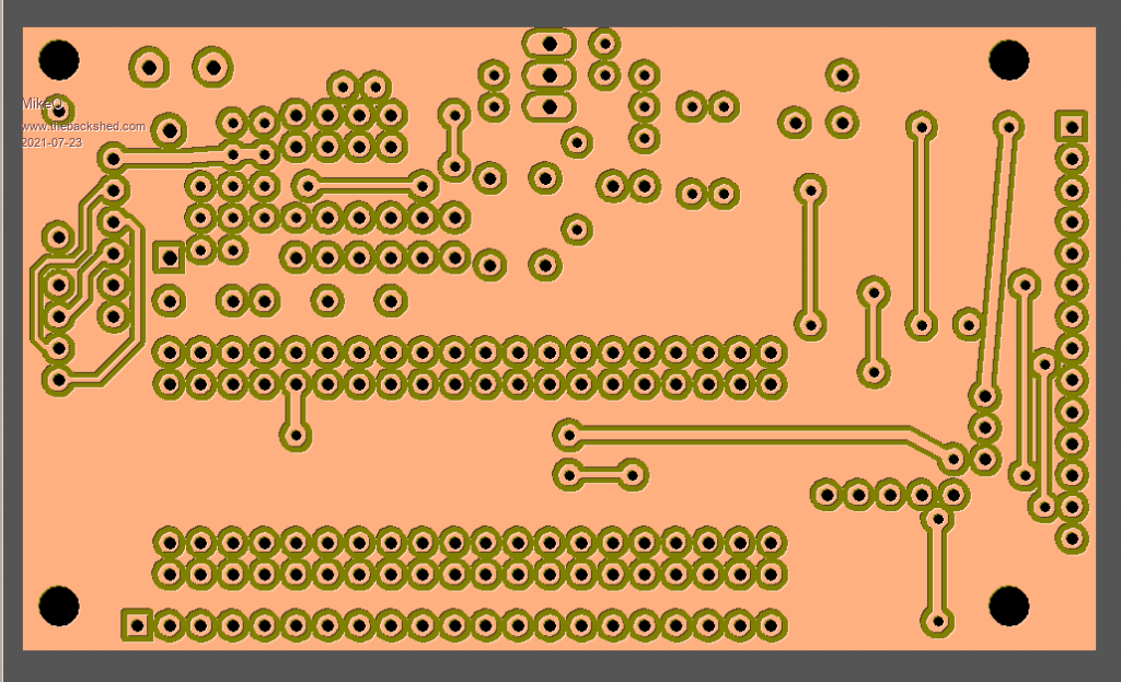 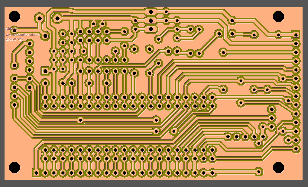 Codenquilts |
||||
| Mixtel90 Guru Joined: 05/10/2019 Location: United KingdomPosts: 5735 |
Although never originally intended to be milled, it looks like a pretty good design for it. :) Please let us know how you get on. Mick Zilog Inside! nascom.info for Nascom & Gemini Preliminary MMBasic docs & my PCB designs |
||||
| vegipete Guru Joined: 29/01/2013 Location: CanadaPosts: 1082 |
Looks neat in virtually milled copper. Should be easy enough to deal with non-plated through holes. I notice a 'milling error' near the bottom right of the (mirrored) bottom layer: 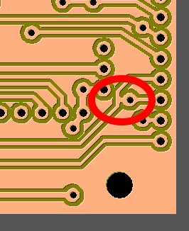 Visit Vegipete's *Mite Library for cool programs. |
||||
| MikeO Senior Member Joined: 11/09/2011 Location: AustraliaPosts: 275 |
Hey your right, thanks I will look at that. I am just at the moment making a new Jig and hopefully a workable "procedure" to deal with the usual problem I have of milling the other side which is always a problem. However I did actually a very successful run yesterday as far as the milling was concerned, ignoring the screw up!. Actually that error you noticed is right under that wayward board cutout move! I have attached a photo. More runs hopefully today. 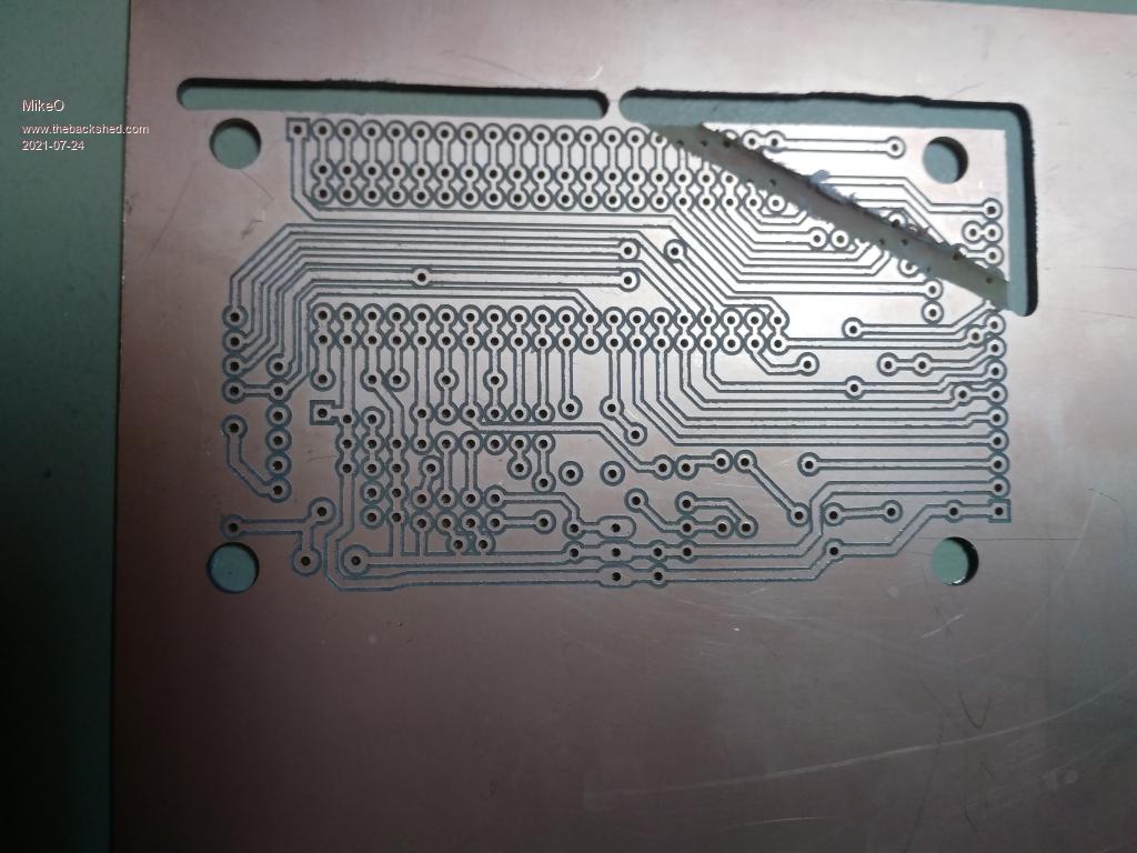 Codenquilts |
||||
| Mixtel90 Guru Joined: 05/10/2019 Location: United KingdomPosts: 5735 |
AAAAARRRRGGGHHH!!!! One of those moments when impolite words pass your lips and you run the risk of not being allowed into Heaven. :( The milling looks nice though. Mick Zilog Inside! nascom.info for Nascom & Gemini Preliminary MMBasic docs & my PCB designs |
||||
| Volhout Guru Joined: 05/03/2018 Location: NetherlandsPosts: 3555 |
@mikeO, Check your milling, the IO0 and IO1 on the ESP8266 are shorted to the nearby trace. Volhout PicomiteVGA PETSCII ROBOTS |
||||
| vegipete Guru Joined: 29/01/2013 Location: CanadaPosts: 1082 |
Well spotted, I didn't see 'em. Those would be a short to ground. 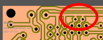 Visit Vegipete's *Mite Library for cool programs. |
||||
| MikeO Senior Member Joined: 11/09/2011 Location: AustraliaPosts: 275 |
Yes I spotted that myself this morning, then I saw your post. Actually I was able to manipulate the relevant track width and the adjacent pads a little in CopperCam to deal with the transgression! I have been using this PicoMite backpack board as an exercise in PCB milling. Actually I am impressed with this latest version of CopperCam, I have had a licence for it for years and its fair to say I had not found it very successful but there has been regular updates to it and now it is working pretty well and consistently. I have made a several isolation milled PCBs previously but they had created from scratch with Diptrace for design routing (using design rules and template optimised for milling) and export to gerbers but in the case of this board as I only had access to the gerbers I could not optimise in Diptrace but non the less CopperCam has done a good job. I have also found that using the registration holes (0.6mm drills) feature in the software not for mechanical location via pegs but rather using the camera on my mill to locate XY for each side. This method has given me a simple and effective double sided board alignment. Today I will try a new run incorporating all these things I have learned , let you know how I go. Mike Codenquilts |
||||
| MikeO Senior Member Joined: 11/09/2011 Location: AustraliaPosts: 275 |
Here is the finished PCB, it has turned out really well so I am very happy with the effort put in and confident I have put some consistency into my process. Thanks again to Mick and Vegipete for the design and Gerbers. Just have to populate and test it tomorrow. Mike PS the small damaged portion on the first board (RHS) is just where the hold-down tab was and I was not careful enough when removing the board from the jig. 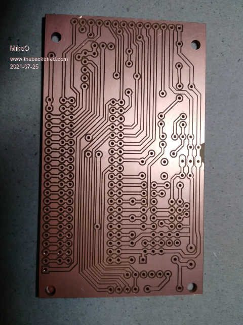 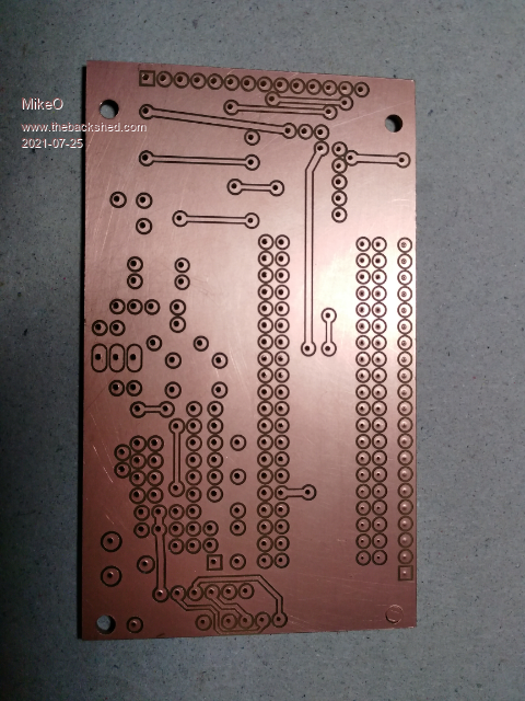 Codenquilts |
||||
disco4now Guru Joined: 18/12/2014 Location: AustraliaPosts: 844 |
Hi Mike, Any tips on what bits and drill sizes you used for this. Like a few others I have just got a CNC kit and about to try a first board so interested in any tips you may have. Regards Gerry Latest F4 Latest H7 |
||||
| MikeO Senior Member Joined: 11/09/2011 Location: AustraliaPosts: 275 |
Hi Gerry, For drills I usually use 0.6mm for Vias and most surface mount components. For connectors, dips etc I use 0.9mm. Mounting points 3mm. I try to limit the drill sizes if its just the odd one you can always just open them up a bit manually. For engraving I use a 3.175mm V engraving bit, 35 degrees. I cut 0.9mm deep and run at ~ 24000 rpm. I have found that a fine spray of WD40 on the top of the board when you start off helps to keep the cuts clean. The other really beneficial addition if your system allows it is surface level compensation , I don't think I could support the depth of cut I use without it. What kind of mill do you have. I can elaborate on my system and process if you or others think that would be helpful. Mike Codenquilts |
||||
| MikeO Senior Member Joined: 11/09/2011 Location: AustraliaPosts: 275 |
This is a file I have found useful for testing when you seting up and optimising your mill. it has an assortment of track sizes, pads etc . The one I did on my system is missing output to the right as I was running out of material. test1.zip  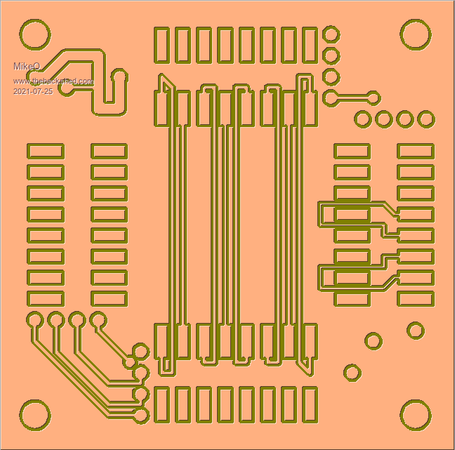 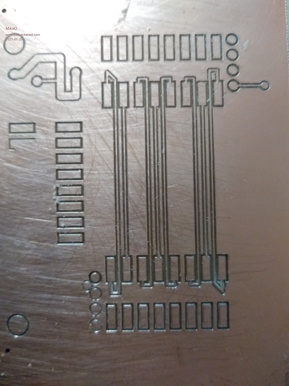 Codenquilts |
||||
| disco4now Guru Joined: 18/12/2014 Location: AustraliaPosts: 844 |
Mike, Thanks for tips. I have 3018 Pro 3 Axis Mini DIY CNC Router Adjustable Speed Spindle Motor. It allows mapping of the surface. This is picture of it This is the thread that kicked off the impulse/lockdown buy. Gerry Latest F4 Latest H7 |
||||
| lizby Guru Joined: 17/05/2016 Location: United StatesPosts: 3017 |
I haven't yet received my CNC router, but I also would like to gather any tips about how to set it up and use it. I like your sample PCB with traces run between pads. That seems fairly necessary to me for moderately complex boards, though Mixtel90 did very well without them. PicoMite, Armmite F4, SensorKits, MMBasic Hardware, Games, etc. on fruitoftheshed |
||||
| Mixtel90 Guru Joined: 05/10/2019 Location: United KingdomPosts: 5735 |
Wow... that's some neat and very precise milling :) Mick Zilog Inside! nascom.info for Nascom & Gemini Preliminary MMBasic docs & my PCB designs |
||||
| MikeO Senior Member Joined: 11/09/2011 Location: AustraliaPosts: 275 |
Sorry I did not intend to hijack this thread but a couple of you have mentioned they would be keen to hear of my experiences I can share, so here goes. My Milling system which I have had several years was not particularly cheap but I paid more to ensure I got a unit with a heavier construction like 20mm support shafts and helical drive rods. The original unit had a parallel interface which has since been updated to USB. Apart from PCB milling I have produced items in wood and plastic (mostly acrylic and HDPE), I have done very little metal milling work with this mill. 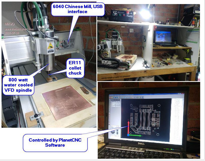 I have had mixed success previously milling PCBs , I could usually get reasonable milling results as long as I stuck to the things I knew to work and took no short cuts. the biggest problem area I had was having a simple and reliable method to deal with double sided board alignment. With this last board I did I was determined to try and solve this dilemma. I will get to the seemingly simple solution in a moment but first I will just list the hardware and software tools I use. 1. Chinese 6040 mill, PlanetCNC (Lic) USB controller and software. 2. General cad work I use CamBam (Lic). Use this for board cutout when doing PCBs. 3. PCB design I use DipTrace (free), I am use to this product, works for me. 4. PCB Gcode I use CopperCam (Lic), I can also export gerbers directly from Diptrace into PlanetCNC but the CopperCam gives a lot more flexibility including origin alignment options. FlatCam would be the other contender (free) I have tried some time ago, always seemed complicated but the most recent looks more streamlined. This time I wanted to try and address the double sided alignment issue. I came across a jig where you milled a xy straight edge on a base board that was reliably located by the addition wood strip against the tables front edge. This meant in future the jig could be reliably remounted with a milled xy edge for the pcb blank to locate on. Secondly instead of using the usual registration method of pins through the pcb into the base board to allow the board to be turned over and located again I used 0.6mm drilled holes at the bottom of the pcb. These can be created in CopperCam in my case other wise they would have to be created by the pcb design software as they need to be registered as machining origins in the gerbers. These photos show the process. Create the Top and Bottom nc files using the left and right reg hole as origins respectively. .jpg) .jpg) On the CNC with the Top.nc you use the zero XY as set. Then when you flip the board over you need to align the zero XY to the LH reg hole (actually the RHS reg hole in the bottom.nc file) .jpg) .jpg) In a previous post I missed a zero It should of course have read: I cut 0.09mm deep So to recap: For engraving I use a 3.175mm V engraving bit, 35 degrees. I cut 0.09mm deep and run at ~ 24000 rpm. I have found that a fine spray of WD40 on the top of the board when you start off helps to keep the cuts clean. The other really beneficial addition if your system allows it is surface level compensation , I don't think I could support the depth of cut I use without it. I hope I have covered everthing, Mike Edited 2021-07-26 19:40 by MikeO Codenquilts |
||||
