| Menu | JAQForum Ver 19.10.27 |
| Menu | JAQForum Ver 19.10.27 |
Forum Index : Electronics : Turning a Toyota Prius into a "portable" generator
I have carefully mulled over your circuit diagram (from a stepinverter link) Your solution is so elegant!! I can really appreciate the simplicity of this design. I am modifying an old dick smith eeprom programmer kit k-3602 (i found an old computer that still has a parallel port -there are many unusual object in my rambling workshop) that can be modified to program up to 128k x 8 ...but not 256k x 8 That would be half of your 256 rom.. I still think that could work, but the rom tables would just be a little more spaced out but still run from 50% to 100%..maybe slightly less smoothly. I have included an altered schematic below that I think would still work within the limitations of my eeprom programming ps. With my lower system voltage, i will be doing my own isolated power supplies (36v--> 12v) for the optos or using your idea of stepping up > 60v and using those cheap chinese converters to step down with isolation(prob 12v with the FOD3182 's) cheers simon 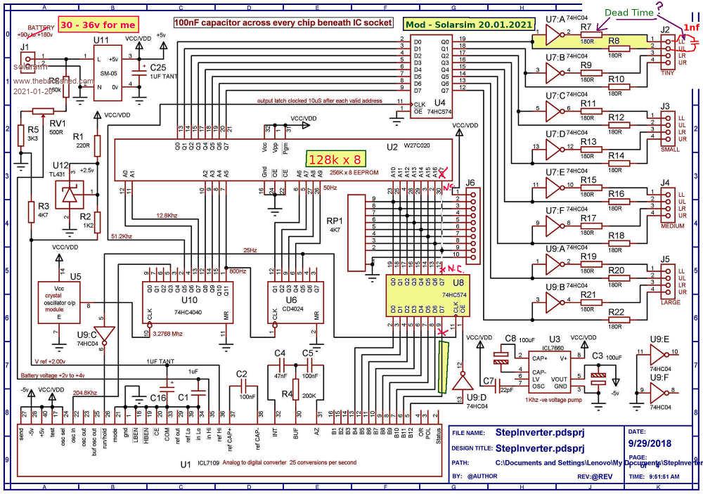 |
||||||
Righto gents, I've received another 25 victims from Digi-Key. (IGBTs) A moment's silence for those IGBTs that have fallen in their line of duty to this point. Let's hope the slaughter does not continue. To recap, I think there is a voltage transient that is killing the IGBTs when they are switching, possibly due to some line inductance. They are working at 140v, but failing when driven at 320v. These next IGBTs are 650v rated. The only way to prove what's going on is to get an oscilloscope and high voltage probe, and they are on their way and should be here next week. I'm going to try slowing down the switching speed, and also adding low value caps right at each igbt pair. The aerosharp has this 1uF cap at the igbt input. I wonder if that's what I'm missing. 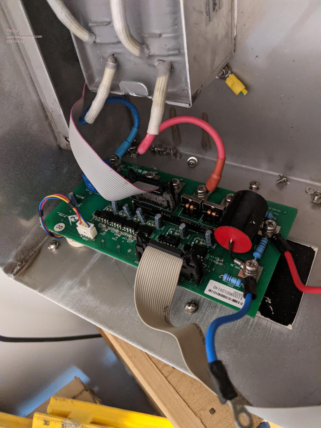 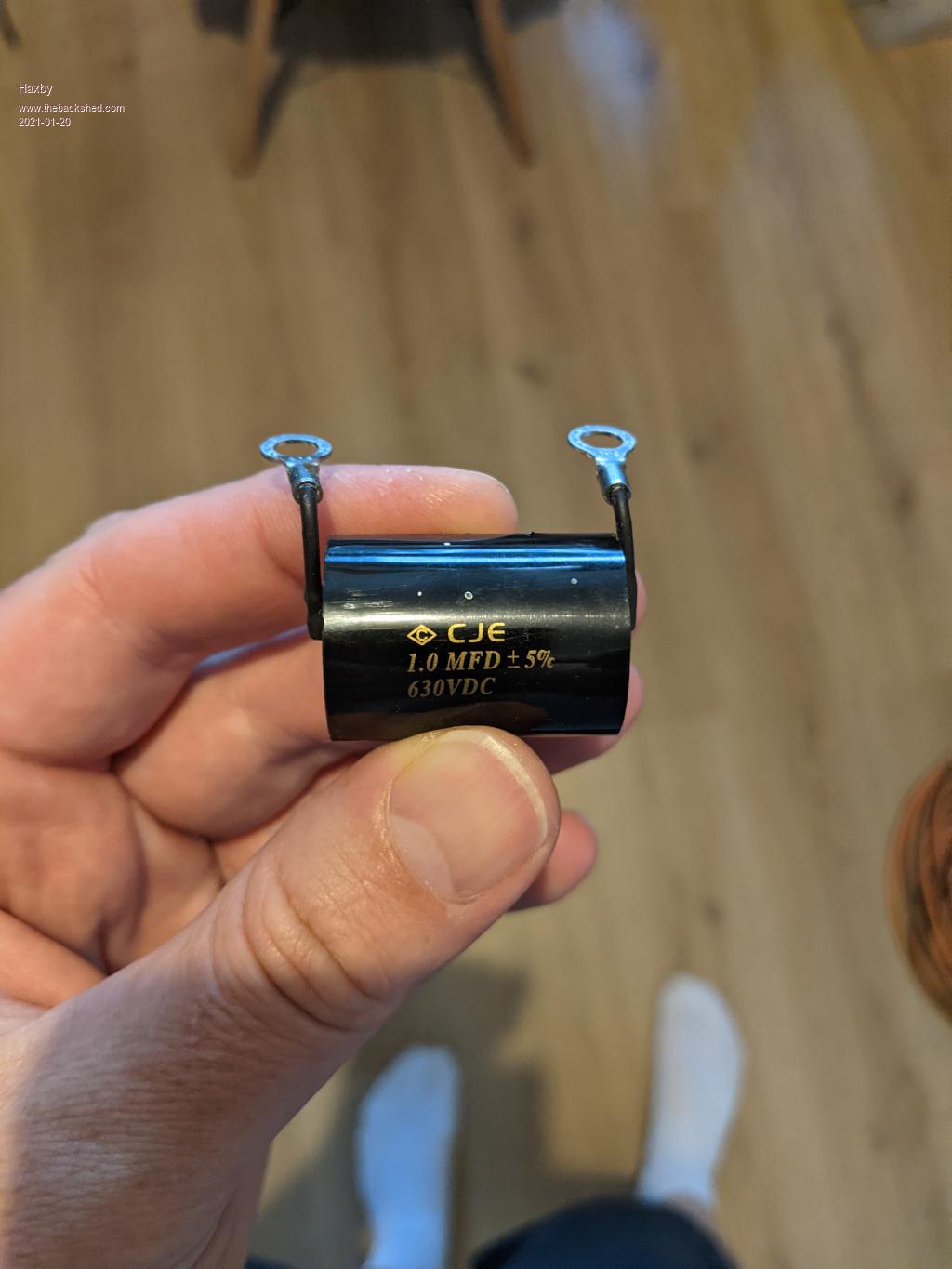 What type of capacitor is this? Metal film? Jaycar has 630v rated greencaps. Would they be ok as a substitute? If so, I'll pick some up tomorrow. |
||||||
Phil, Usually those monster pulse rated capacitors are polycarbonate, and excellent devices. An oscilloscope is going to be extremely helpful in finding the cause of your problems. Simon, That should do very nicely. Half as many lookup tables will work very well for you, 256 is really overkill. For dead time 1nf = 300nS which will be fine for mosfets. 10nF = 2.5uS for big old slow IGBTs Voltage divider R5 and R6 will need to be changed for +2v to +4v coming out of the pot for 30v to 60v incoming dc. I can supply a circuit board, but don't know how that would go with a smaller rom that may be have a different package and pinouts. There are a lot of power supply decoupling capacitors not shown on the schematic, I ran out of physical space on that A4 sheet to include them. Edited 2021-01-20 20:23 by Warpspeed |
||||||
Thanks warp, the DSO is coming today. I'm also going to try a RC snubber circuit between emitter and collector. The calculators for selecting the values of R and C all expect a switching frequency, which isn't fixed in our case. Any ballpark figures to try first based on your experience? If not, I'll just get a handful of greencaps and (wire wound?) resistors and experiment. 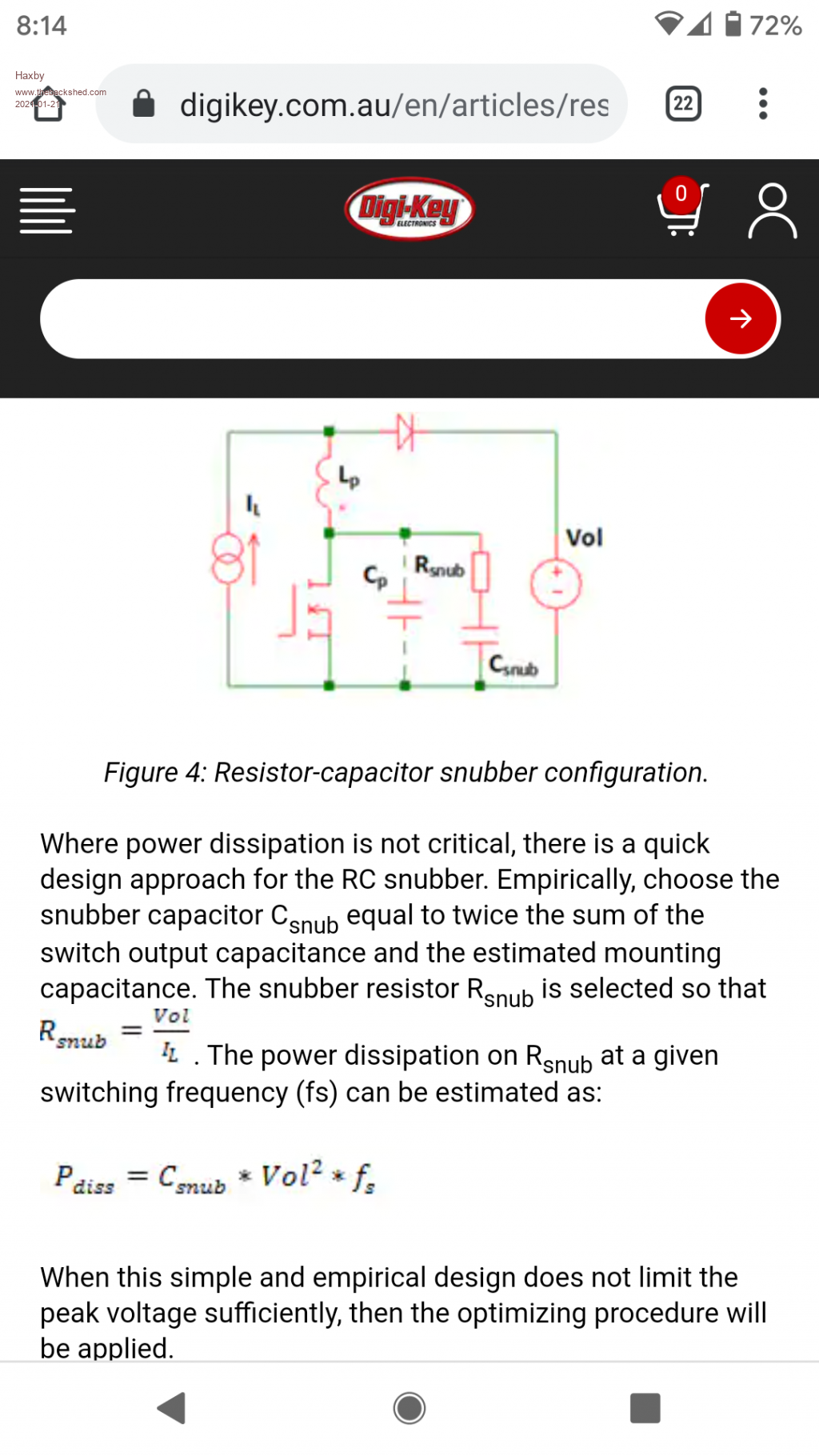 |
||||||
There is no simple answer to designing a snubber, it depends on what the purpose is, and what its supposed to do. Various reasons for designing a snubber, but the usual function is to reduce the rate of voltage rise when something turns off. You also need to consider what happens when that "something" turns back on again. Simplest snubber might be placed across switch contacts operating at a high dc voltage. If the contacts physically separate faster than the voltage is allowed to rise, there cannot be any arcing. Placing a very large capacitor across the contacts will achieve that. Unfortunately the capacitor charges up, and when the contacts close again, we get a big splat which welds the contacts. So we fit a series resistor to limit the current. Diodes can be useful here too. We can have different resistors for capacitor charging/discharging, and various snubber circuits can be designed to have more ideal characteristics, depending on what its supposed to do, and the time intervals involved. We can do the same thing with a transistor, mosfet, or IGBT. Restrict the rate of voltage rise sufficiently so that turn off switching losses in the device can be reduced, or eliminated altogether. Total losses will be much higher though. But the switching losses can be transferred from the switching device to a high powered resistor, which may be an advantage. In our case with IGBTs switching at a very low cyclic frequency, switching losses are going to be negligible. Big difference between tens of Hz, and tens of Khz. Half bridge topology also clamps the voltage very effectively between ground and the positive supply. I cannot see what advantage a snubber is possibly going to offer in this situation. Decide what you want the snubber to actually do, and then work out some suitable values which will depend on the required rate of voltage rise, the current the snubber must carry, and the voltages involved. Your oscilloscope is going to be very useful for monitoring snubber operation. |
||||||
Oscilloscope arrived! Isolated HV probes will be a while. Testing on the lower igbt at 150v I got this yellow trace. (Blue trace is power supply): 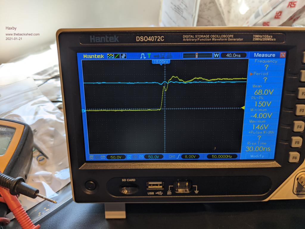 Looks terrible! And that's with no transformer connected. Then I added a 1uf cap right at the igbt pair on the power supply rail: 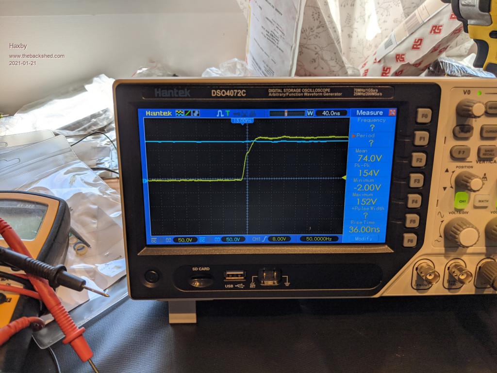 Looks a lot better ... Still a bit of a shoulder there. |
||||||
That all looks perfectly o/k. |
||||||
Thinking about that a bit more, its the least significant bit you need to eliminate, not the most significant bit. |
||||||
Something I'm surprised about is that the igbt gate driver trace looks a lot slower than the HV transformer output trace. Both are pretty quick, but is that a concern? 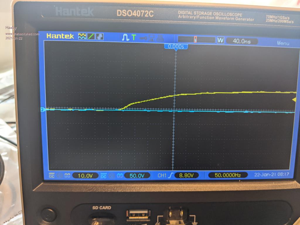 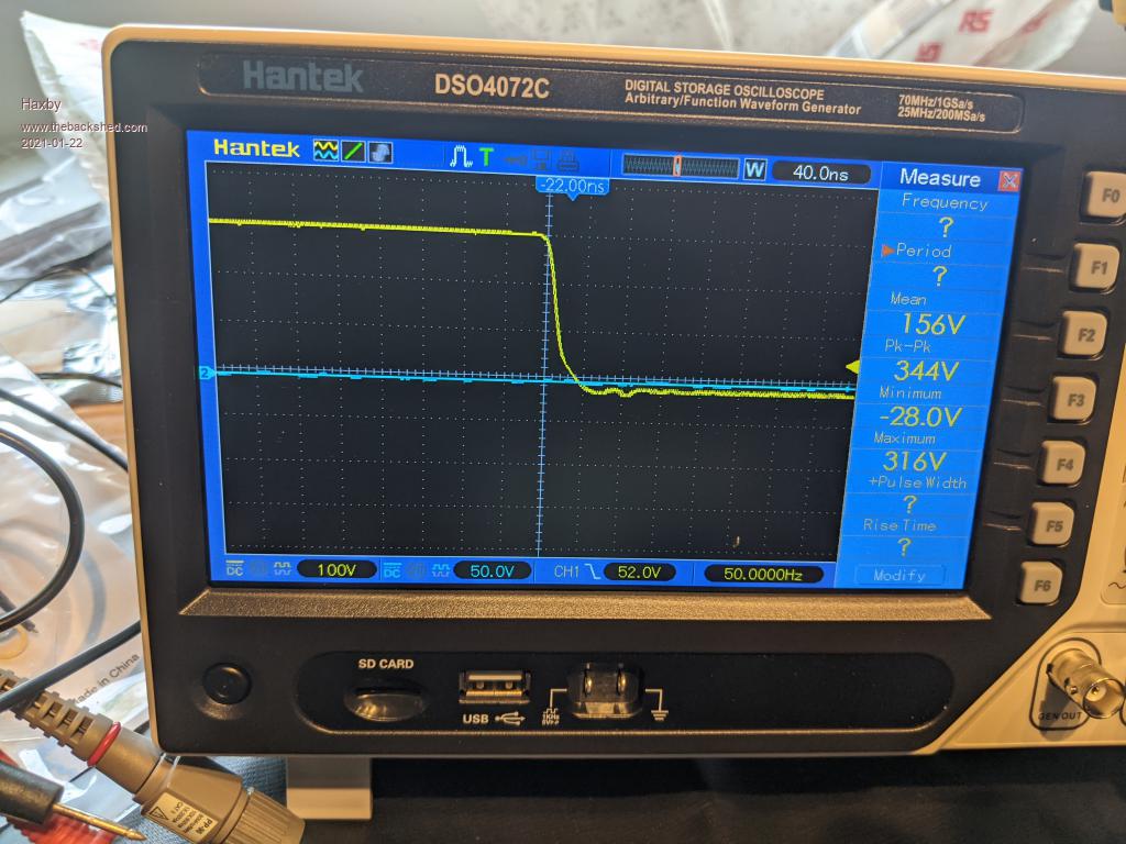 |
||||||
The IGBTs have a LOT of gain, so hardly surprising really. |
||||||
More atrocities but maybe some light at the end of the tunnel: After checking all gate driver ICs and rebuilding the igbt board, and buoyed by yesterday's success in smoothing out the newly discovered terrible power rail fluctuations with the addition of 1uf capacitors, I was quite confident that the culprit that blows the IGBTs was found. The 1uf caps really smoothed out the terrible power supply spikes in one of the inverter stages, so the addition of 8x 1uf caps was made today. One for each of the half bridges. Little did I know that the capacitors may have masked an even bigger problem..... So today I connected the transformers and slowly increased the voltage again, as I had done many times before. I was more confident today though, as the new oscilloscope was showing me an in depth view of the output, the power supply fluctuations were gone, and everything was looking good. But.....Ater passing 200v, again a familiar pop was heard, my heart sank, and two more IGBTs met their maker. Pausing to think for a moment, I realised that one thing I have not measured to date is the gate voltage trace while the high voltage power supply was on. I have been using two power supplies; one 1A 80v supply that runs the warpverter board with gate driver ICs, and the other one runs the high current section of the board. This is to safely poke and prod the gates, igbt driver ICs and logic circuits without having up to 400v on the board... So I moved my focus to the next inverter section, with fresh new IGBTs, and connected one DSO channel to the gate, and the other to the source. Then I turned up the voltage while scoping the gate voltage. Well this is another great clue: the gate is bouncing like a trampoline, and as I turn up the high voltage, that big dipper gets way worse. And that's only at 50v or so. The DSO is really earning it's keep. But what could be causing this bouncing? 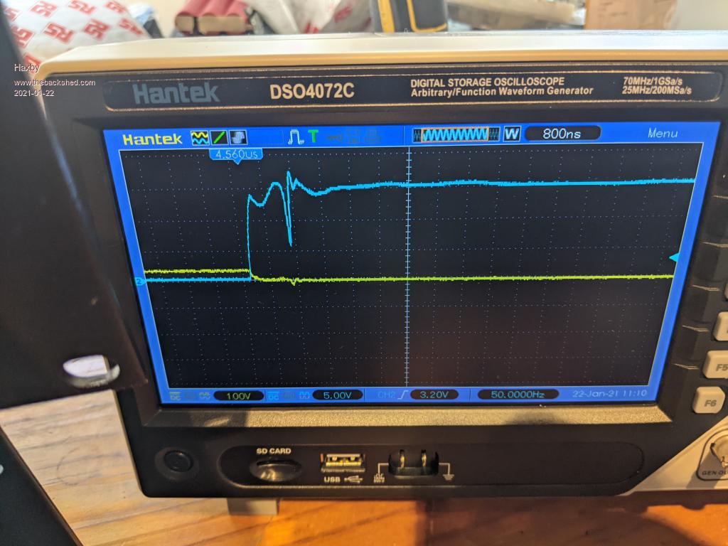 |
||||||
I'm still driving the gate with a 10 ohm gate resistor. |
||||||
That negative spike is probably capacitive coupling from collector to gate. See if it coincides with the negative going collector voltage. |
||||||
The source voltage is shown in yellow (100v per division so about 50v). Is that what you mean? It's not in line with the source voltage falling. |
||||||
That looks like parasitic oscillation. Usually caused by stray inductance. Increasing the gate resistance will help, but reducing the stray inductance is there so fix. |
||||||
Stray inductance? I wonder where the inductance is? There is no transformer connected on the output. |
||||||
Stray inductance in the driving circuit, not the output circuit. It is possible for the inductance in the gate path to combine with the capacitance of the FET/IGBT and form an LC oscillator. Like here: https://toshiba.semicon-storage.com/info/docget.jsp?did=59456 |
||||||
Hmmmm, not much can be done to decrease the gate inductance. The gate driver opto, decoupling caps, and gate resistor are all in a small footprint. The isolated power supply is right there on top of them. I drew in the underside tracks for clarity. I'll increase the gate resistance next. 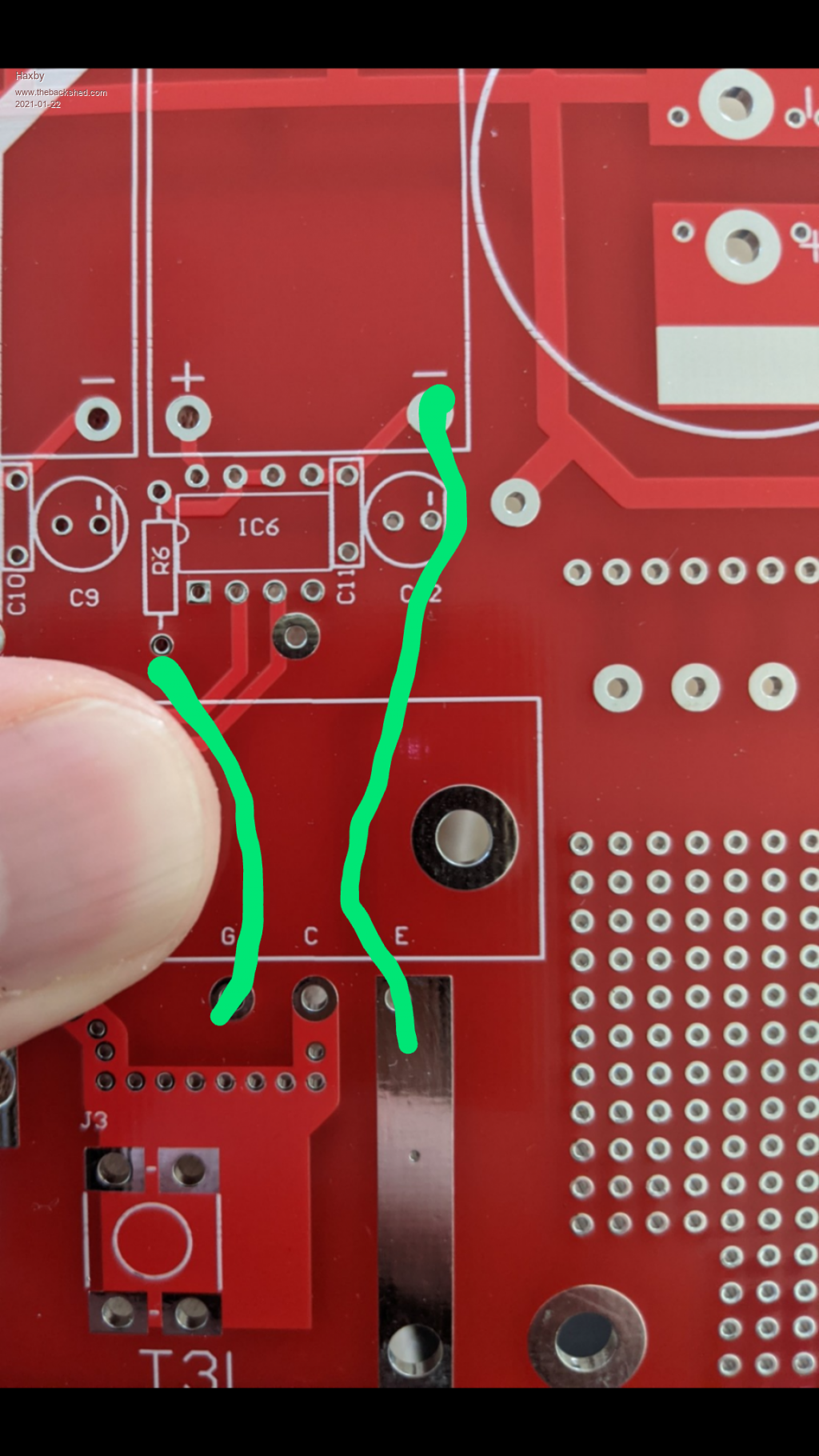 |
||||||
It's possible the voltage dip is not the cause but more the result, it looks like 20V, that's a lot, maybe adjust the voltage resolution to get a beet view. Its'proably wise to swap your channels/probes, there could be a delay between channel 1 and 2 of your scope and maybe not completely synchonized. I did a small test with the internal generator o my scope, but could not reproduce what I said. So it may be tricky to make a good conclusion, keeop in mind the mosfetdriver is adding a delay as well, not important for this measurements thoubh. If you measured that gate signal on the igbt itself, then that's a verry fast turn on. It looks like you are switching it under 100ns. In a previous scoop image without transformer I saw it was on in about 40ns. When the gate of your igbt is reaching 4-5V it will be already completely turned on. To make it slower you can raise the resistance of that gate resistor and/or add some capacitor between gate and emittor to make it less sensiive and slow down the speed even more. Before I sad your gate wires are looking long to me, others do not agree. I still believe they are too long for the crazy fast turn on you have now. EDIT Are they close to a parallel current carrying track?, If so that's not good, it will influence your gatedrive. What you can do is driving with twisted wires to gate and emittor to see if it has some positive effect. Maybe not so important now, but it can become a problem under load. Oh, not yet a transformer connected. I would make sure you can measure those dead times. You are now measuring the low side IGBT? Edited 2021-01-22 18:21 by nickskethisniks |
||||||
Yes this is the low side igbt. Yes it's definitely switching at 40nS. I can increase the gate resistor from 10 ohms to 100 ohms. What is a good switching speed to aim for? Sounds like the high voltages I'm using are increasing the capacitance coupling issues drastically. The measured dead time between low side and high side gates is a very slow 2.5uS so I have plenty of wiggle room, except for the heat dissipation, which isn't an issue just yet. |
||||||

