| Menu | JAQForum Ver 19.10.27 |
| Menu | JAQForum Ver 19.10.27 |
Forum Index : Electronics : Turning a Toyota Prius into a "portable" generator
You can aim for 0.5-1uS for the big inverter, it's possible you don't need to be that slow but you can try with 100R and see where you get with that. It will probably still be fast. I think it's also wise to probe your 12 or 15V on your mosfetdrivers, so you can rule that out. When driving a mosfet verry fast you need to be sure this voltage is good quality. You allready have a ceramic and electrolytic capacitor close to your driver so this will not be a problem. I did have simular but not so bad gate drive without the electrolytic, it looked like more like a damped oscillation. I read on another forum that regulated power supplies for gate drivers could create problems as well, but this was more problematic with verry high current motor inverters/drivers. The voltage regulating loop could become unstable and then it is better to use unregulated power supplies. But here, this will not be the case a guess. Edited 2021-01-22 20:16 by nickskethisniks |
||||||
Interesting points. Thanks for your time. I'll try the 100 ohm gate resistor tomorrow and go from there.  |
||||||
You can certainly try a hundred ohms, or even more, and it may work very well. But just remember that this is potentially going to be a high voltage system, and capacitive coupling between collector and gate may start to become significant if you drive the gate from a much higher impedance. I also suggest you test your IGBTs for high voltage breakdown as suggested earlier. Short the gate to cathode and run the collector voltage up to 400v, or whatever. It is almost certain to be o/k, but if your IGBTs are breaking down and failing at say 80v, you are wasting your time pursuing other possible causes. |
||||||
Blue trace is measured at the gate. (Vge) Yellow trace is measured at the collector (Vce). This is with a 100 ohm resistor. The big dip at the gate is gone. The gate still wants to switch on very very quickly! 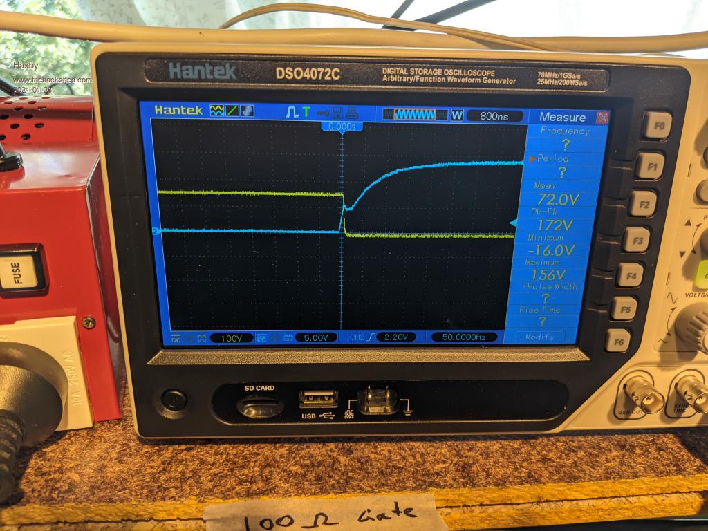 |
||||||
The gate voltage initially rises very fast, before the IGBT begins to conduct. As soon as conduction begins (in the linear region) the collector voltage drops like a rock. That capacitively couples into the gate, and tries to force the gate negative, fighting the gate driver and series gate resistor. Once the IGBT has turned on, the collector voltage is no longer falling, and the gate is free to rise further. That all looks fine, nothing wrong there. About three divisions later the upper IGBT should turn on. |
||||||
The light at the end of the tunnel is looking brighter: All this focus on the turn on time detracted me from looking at the turn off time. Turns out there were terrible things happening there too! With the 100 ohm gate resistor, the turn off time at the gate looked like it was approaching too close to the 2.5 uS threshold. 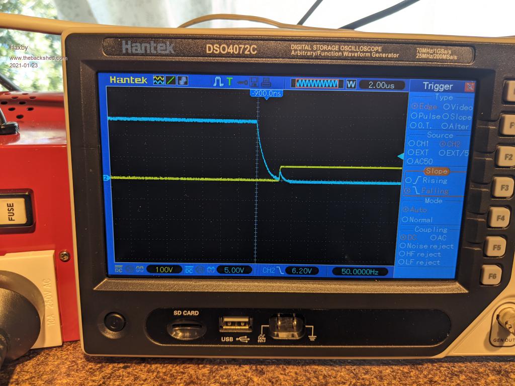 You can see the blue gate trace taking its sweet time to turn off, then it gets pounded by the high side igbt quickly turning on at the 2.5uS mark. I added a diode and 10 ohm resistor to the gate drive to turn off quicker, but still under control. That sorted out the turn off shenanigans. Another problem now discovered was that there was a giant dip in the gate drive that was appearing seemingly out of nowhere, but always in the same position well into the square wave..... That turned out to be transients from the high side igbt switching. While mucking with the low side gate, I realised that I should be copying everything I'm doing to the high side igbt. Finally in an attempt to slow down the 40nS very fast switching, I added a 100nF capacitor between gate and emitter. This slowed the switching time to 200nS. Still very fast, but I'm reluctant to add more capacitance because the gate voltage trace now looks quite spongy. The following are the latest traces of the Vgs and VCS, two pics just with different time bases, and I think I'm ready to increase the voltage and see if there are any more fireworks! What do you think? What are the unintended consequences of such a spongy gate voltage? 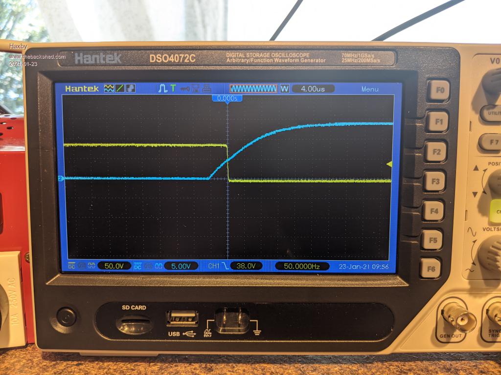 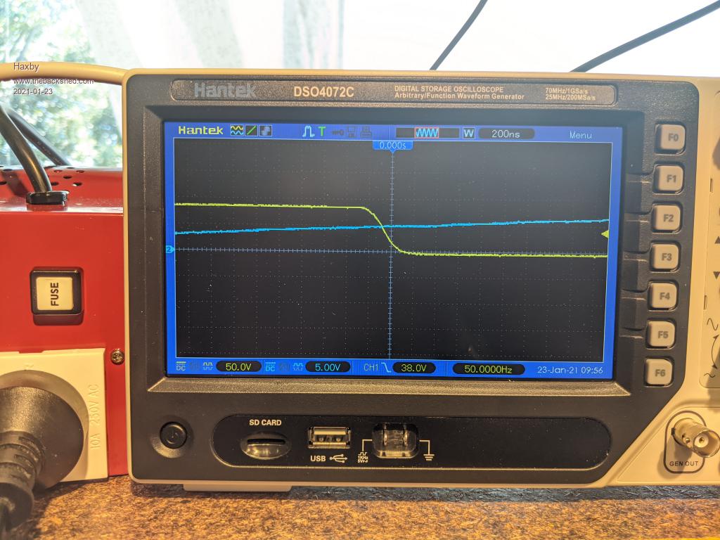 I chose these IXGN75 and IXGN90 IGBTs primarily because the tabs were insulated. I saw that they were fast turn on, and didn't think this would be a problem, if anything, it would be an advantage due to lower switching losses. In hindsight, I would have chosen some older slower IGBTs, as that's basically what I'm converting them into with the added gate caps. |
||||||
See how it goes. Very slow switching means higher switching losses, but as its only 50Hz that should not matter. It will probably look quite different with an inductive load and higher dc voltage. |
||||||
I've just realised that the extra gate cap slows the turn on time to 4uS from when the driver IC is commanded to turn on, to when the igbt conducts. This is only ok if the turn off time has a similar delay. And only ok if that stays that way in any dynamic environment (temperature, inductive load, etc) So I'll decrease the gate resistor a little bit for more headroom. This is turning into a juggling act but I'm gaining valuable knowledge as I go! |
||||||
It can all be made as slow or as fast as you want to make it, but there absolutely must not be any overlap where both IGBTs are on simultaneously. Edited 2021-01-23 13:16 by Warpspeed |
||||||
Currently I have a 10 ohm resistor and fast diode across the gate resistor. This arrangement turns off the igbt gate quickly. If I want to turn off quicker, I can decrease the 10 ohm resistor. Since the driver IC hcpl3120 is rated at 2.5a, I feel that I shouldn't go less than 6 ohms, otherwise the current rating of the chip can be exceeded when discharging the (now substantial) gate capacitance. But I see many designs out there that just have a diode with no turn-off resistor at all, directly across the gate resistor. Are they just getting away with it due to small gate capacitance? Am I missing something? |
||||||
You are quite right, many people do that, but its bad practice. There will be no current limiting, and its pretty tough on the mosfets in the gate driver chip. I used ten ohm resistors and no diode. As you can see from the photographs I posted earlier on page six, I made provision for a diode when I laid out the boards, but none was ever fitted. Edited 2021-01-23 14:38 by Warpspeed |
||||||
Perhaps you could try a gate R of approx 25 ohms, no parallel diode, but place a small cap (470pf - 1000pf) across the gate - emitter of one device and look at the waveform. The small cap will act as a HF filter on the gate, slow the device a little but more importantly help absorb the energy induced from the fast changing collector side. As you are running at low frequencies the extra loading on your driver will be minimal. Cheers Mike |
||||||
I think I have found a reasonable compromise with the following gate drive components: 47 ohm gate drive resistor. 6.7 ohm resistor and diode across gate drive resistor to aid in turn-off time. 82nF capacitor across gate to slow down turn-on time and to stop the gate from being capacitively coupled to an on state when a fast voltage transition occurs at the drain. All that looked good on the DSO, so I attached a transformer and turned up the DC voltage to 250v. Now there is a new puzzle to solve: The transformer is saturating mildly due to a strange offset effect that I captured on video. here The video shows me turning up the voltage on the Variac. At the 30 second mark, I'm up to 250v, and you can see the yellow trace starting to climb from zero, to around 20v. This is enough of an offset to saturate the transformer core, and if you turn up your speakers, you can hear the transformer start to buzz. If I don't turn off the power, the transformer settles down but cycles through this seemingly at random. It only happens at 200v or more. Any ideas? |
||||||
Nothing to be concerned about. You now have rather a lot of dead time, where all four IGBTs in the bridge are going to be off together for several microseconds. During the forced "zero" part of the waveform both lower IGBTs will be turned on placing an effective dead short across the primary of the transformer. That will pull the voltage down hard to ground on either side of the bridge. When you turn off all four IGBTs for several microseconds, the transformer primary just floats up to some random voltage probably determined by stray capacitance and various leakage currents. With the other three inverters also running, there will be current fed back into that primary, and as soon as the IGBT bridge goes into the floating high impedance condition, the voltage will be slammed very hard up or down to either the +ve dc supply rail or to ground, and the voltage will no longer be floating. You will see a very fast and very clean voltage transition between any of the three possible voltage (logic) states on the primary. On the secondary, expect to see some massive voltage overshoot, and possibly slight ringing after each transition. All perfectly normal at this very early stage of running a single inverter and transformer all by itself without any secondary load. Later, as you get additional inverters up and running, the overshoot and ringing and other anomalies, all disappear as the transformer currents become more and more sinusoidal. At this stage, just get all four inverters working properly using the basic 50Hz waveform, its much easier to see what is happening using the simplest slowest waveform. That will also drive any of the four transformers without any prolem. Edited 2021-01-24 16:28 by Warpspeed |
||||||
Warp: Thanks for that.... I worked that out later... I am waiting for a big order of parts now ...could take a while...so doing other related projects while waiting. So: experimenting with simple isolated dual supply for half bridge boards. 30-40 volts to isolated 15dc (x2), (I was thinking 20mA? each). Programming a maximite (k9550) to drive an old eprom programmer (k3602)circa 1994 to program the eeproms w27c20..use 1/2 of Haxby: Ive been reading your posts with interest. That whole concept could have some really interesting spin offs as more ev's hit the road and the 2nd hand market expands... |
||||||
|
||||||
Gents, just a quick update: After learning about, and witnessing, the surprisingly large coupling effects of high voltages on the gate traces, I decided to add TVS diodes to all gates, so I had to pause the build till they arrived. They arrived today, so I'll be working on the project this week. While I was waiting for the TVS diodes to arrive, I was checking all gate drivers again and for the second time I found a gate driver IC that was exhibiting strange behaviour. This is the second one I found with the same fault. The ON time is fine but the OFF time is not good. I post this as a word of warning to make sure anyone building any inverter looks at the on/off times of every gate after a fireworks event. Here is a trace of a bad one: 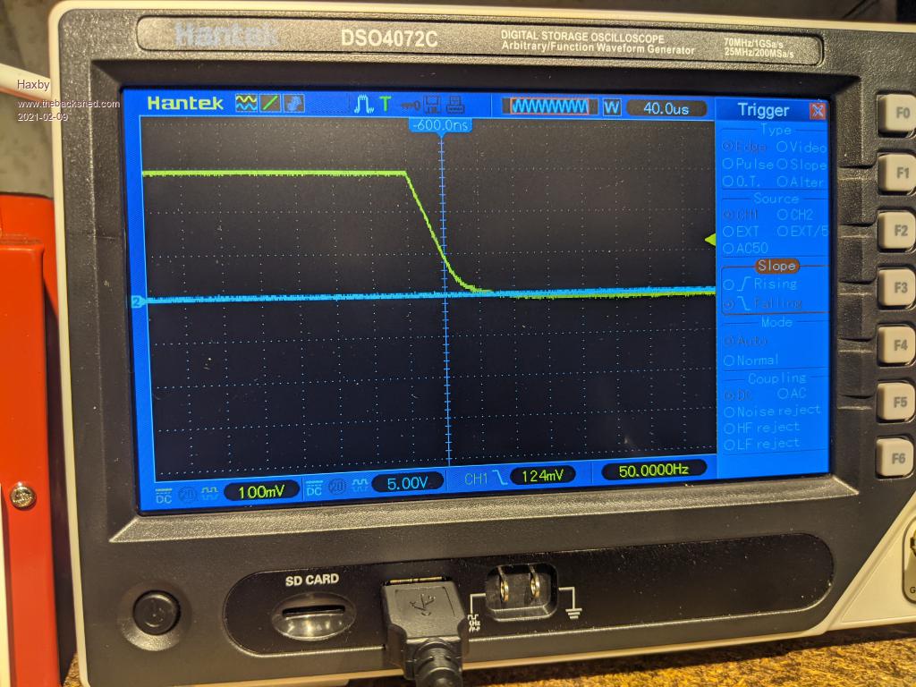 And here is what it should look like: 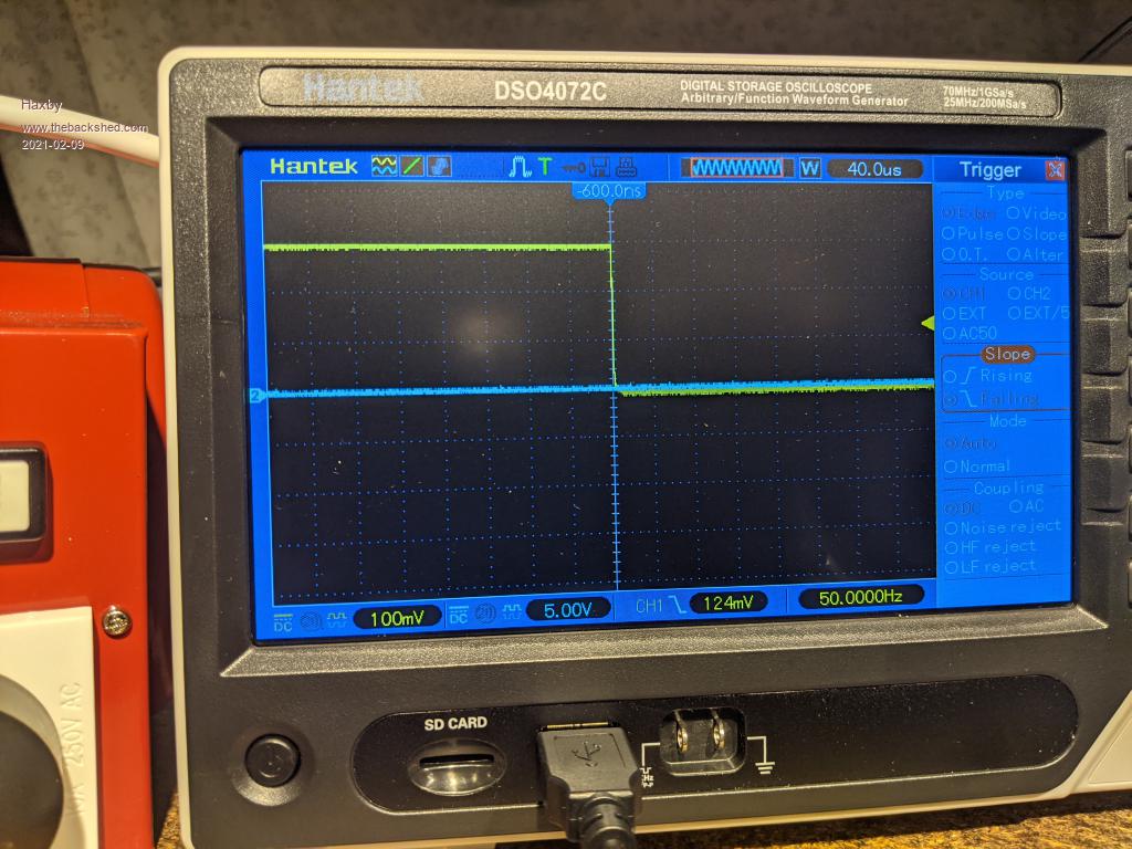 |
||||||
Its not pulling down as hard as it should. Maybe the lower mosfet in the driver chip is damaged. That may be due to the inverse diode experiment, too much gate current being pulled down might have blown the lower mosfet. Its amazing though, faults like this can remain hidden, and the inverter may still actually appear to work. |
||||||
Some good news: I have connected all 4 inverters, and have run at 200v for some time without blowing any IGBTs. Aaaand, I've got 230v RMS out! I haven't yet connected a load to the output. There is still an occasional resonant hum that comes and goes from the transformers. Not sure why. It could be that I'm getting the DC input from a half wave rectifier from mains which is also at 50hz, and when it aligns with the generated 50hz it may cause a bit of step saturation. Will need to eliminate that soon with a full bridge rectifier. The problem now is that I can see some spikes in the output that correlate to the largest inverter turning on and off: 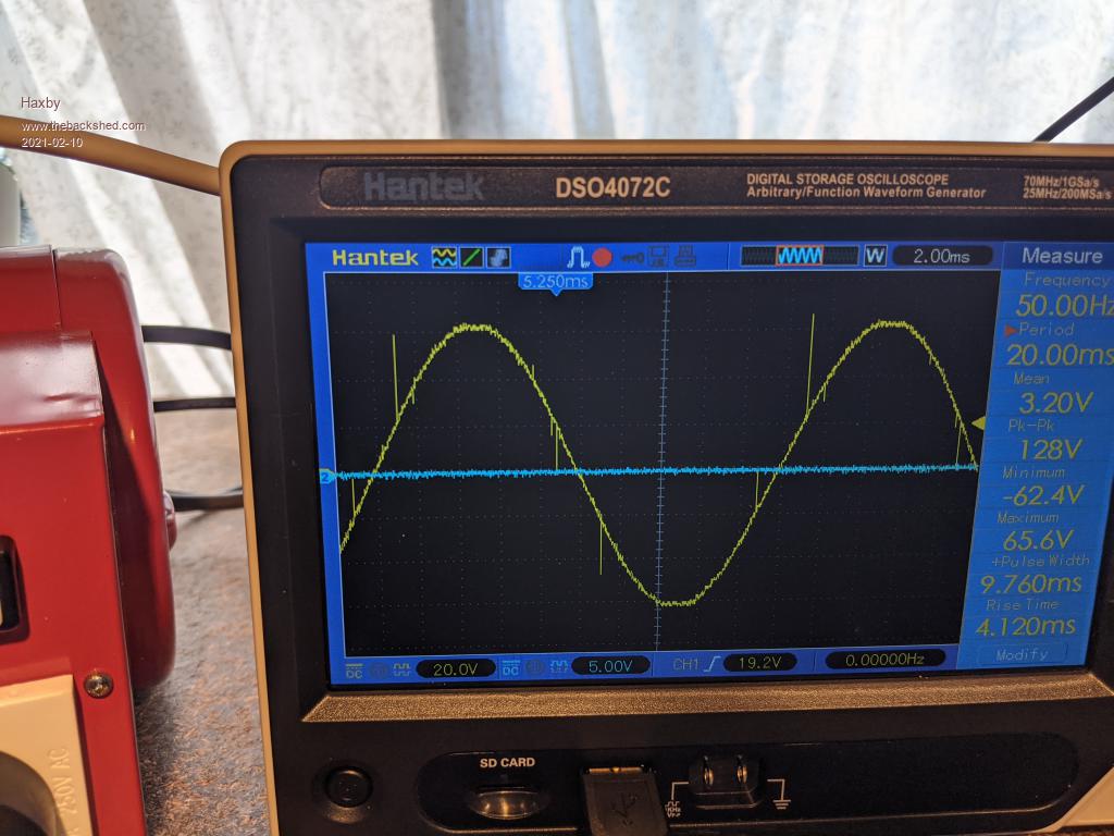 They are not random. The transient pattern is always up then down on the top half wave, and down then up on the bottom half wave. Note that while the divisions say 20v, they are actually X5, so 100v per division. The transients are not on the input square wave side of the transformer, but on the load side. Should I be concerned? |
||||||
No reason to be concerned. There is going to be some capacitive coupling between primary and secondary, and the whole thing is going to be high very impedance on the secondary without any load. Those spikes are going to be extremely narrow, not a lot of energy there to get rid of. An EMI filter and grounding one side of the secondary should make a big difference, and so will some slight load. That is a nice sine wave by the way. |
||||||

