
|
|
Forum Index : Electronics : Various aspects of home brew inverters
| Author | Message | ||||
| poida Guru Joined: 02/02/2017 Location: AustraliaPosts: 1389 |
no sweat noneya The sync function was just something I added that I thought might be good for experimentation or a special case. Honestly, all I want from the nanoverter is an inverter that works for years, and runs publicly available code and can be built by anybody. (I've just got home from 4 days at The Grampians. Lots'a orchids and birds. So that's why I have not replied for a while.) wronger than a phone book full of wrong phone numbers |
||||
| noneyabussiness Guru Joined: 31/07/2017 Location: AustraliaPosts: 506 |
No stress, thank you for all your hard work.. i wish we could get the sync function to work.. its a really great idea. Ive been in and out of hospital for months, back injury thats pretty floored me. Haven't done much for months.. envious of your trip, would have been beautiful I think it works !! |
||||
| noneyabussiness Guru Joined: 31/07/2017 Location: AustraliaPosts: 506 |
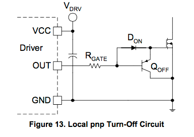
Did you see my post about the local pnp turn off circuit, really good for dv/dt induced turn on.. the app note puts it best, but can be easily implemented on the ozinverter/madinverter boards.. I think it works !! |
||||
| poida Guru Joined: 02/02/2017 Location: AustraliaPosts: 1389 |
No, don't think I saw it. Can you point me to it please? wronger than a phone book full of wrong phone numbers |
||||
| noneyabussiness Guru Joined: 31/07/2017 Location: AustraliaPosts: 506 |
Ok , pics are not working for me for some reason, �its figure 13 on Texas Instruments app note SLUA618A... it will pull down individual mosfets to ground AT the source pin, so as to avoid the driver to mosfet gate inductance... just a thought... I think it works !! |
||||
| poida Guru Joined: 02/02/2017 Location: AustraliaPosts: 1389 |
 I think I will try this and report back the before/after. wronger than a phone book full of wrong phone numbers |
||||
| noneyabussiness Guru Joined: 31/07/2017 Location: AustraliaPosts: 506 |
Thats the one.... I think it works !! |
||||
| poida Guru Joined: 02/02/2017 Location: AustraliaPosts: 1389 |
ok, here is what I get. I am now using the powerjack power board, with custom modules for each of the 4 legs of the bridge. Thanks kentfielddude for making these available and Ben & Amber for sending me some of the small boards. The test situation is: a powerjack power board, driven by a nanoverter, with the IR21844 gate drive IC. On one 1/2 of the bridge, we have 4.7R gate resistors, with 20K pulldowns. One HY4008 per leg of the bridge. All 4 legs have a 220R and 104 monolithic cap snubber. The test 1/2 of the bridge has the modified low side with a PNP turn-off, and a normal high side (4/7R gate and 20K pulldown) All this into my standard transformer and load. I have the capability to see what "normal" is and what "the test condition" is, side by side. In the following, Pink is the test condition, i.e. PNP pulldown and light Blue is "normal", i.e. 4.7R gate and 20 K pulldown. We only look at the gate voltages about in the middle of a 1/2 sine wave. (one 1/2 sine wave is active while the other is just pulling current to DC ground. So the test 1/2 bridge is active for one 1/2 sine wave, then the "normal" 1/2 bridge is active. It's a convenient test setup) Here is the normal 1/2 bridge, under 200W load. There is some shoot through and the low side gate is pulled up into conduction. And when this happens, all hell breaks loose and we have oscillation and coupled responses of various components. 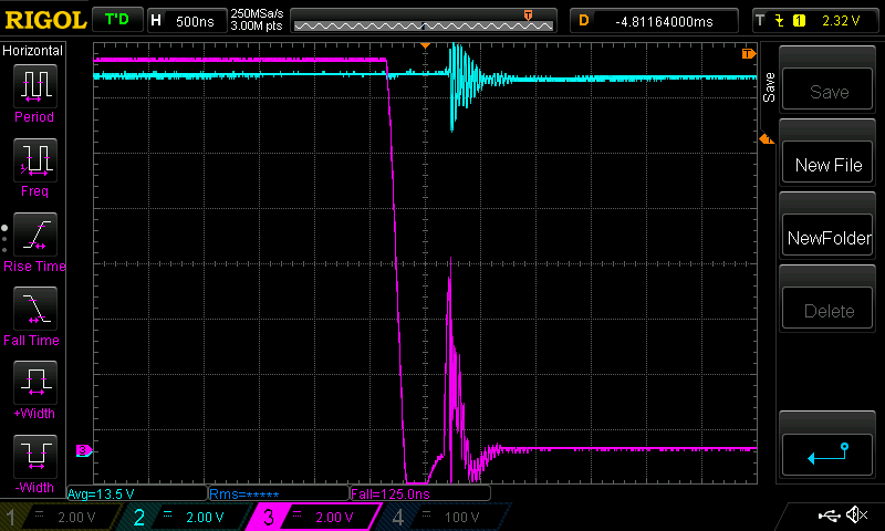 Now look at the PNP turn-off low side gate. 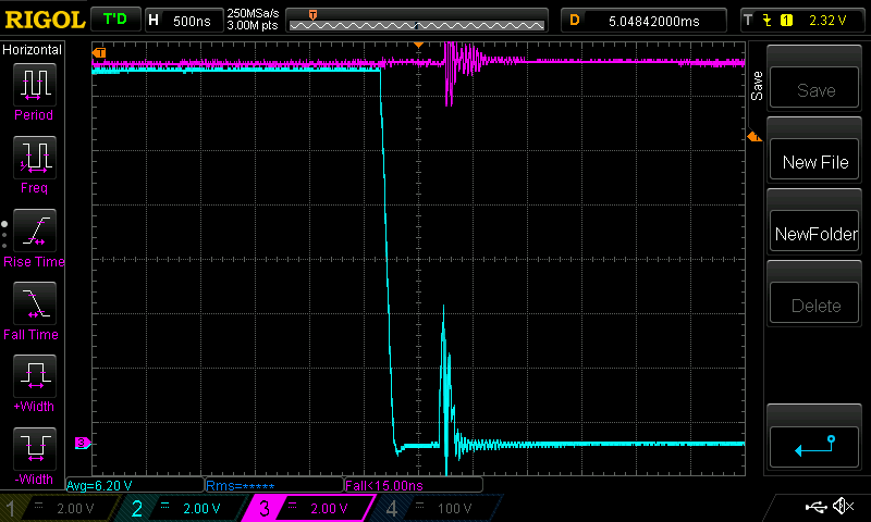 Less ugliness but not great. I would call it an improvement. In this test case, I want to bring to our attention what I see as a primary issue that needs to be looked at: Out of specification gate drive output voltage levels. The IR21844 along with many other gate drive chips does not allow it's output to go below ground by much more than about -0.3V This is where the output drive stage of the IC will start to have a very bad day and just short to ground or Vcc or something. Here is clear evidence that the low side MOSFETs are pulling the IC gate drive outputs below -0.3V, in this case well below, down to about -2.5V I can not expect an inverter to run for long when this is happening. (of course, I need to carefully verify this by probing AT THE IC PINS with good probe technique. I have done this in the past and seen insignificant variation from what I probe and measure at the MOSFET Gate and Source pins. There is a difference, but not much. So what we see here is close to what the IC output pins see.) Pink is "normal" 1/2 bridge low side gate voltage. 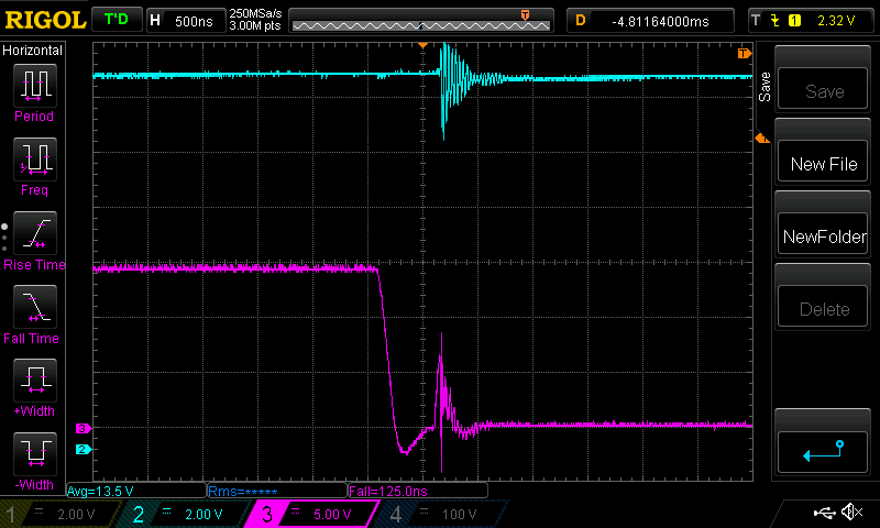 So, when does the low side gate get this unwanted pulse of voltage? When the low side MOSFET Drain rises very quickly, that is, when the high side gate switches ON and pulls the low side Drain (and high side Source) up to DC supply voltage. Lastly here is a capture of the low side gate voltage and the low side Drain voltage. We can see that the gate voltage pulse occurs when the Drain rises a large amount quickly. Light Blue is the modified (PNP turn off) low side gate voltage Dark Blue is the Drain voltage, driven by when the high side MOSFET switches on. The low side gate pulse coincides exactly with the rapid voltage rise due to the high side switch ON. 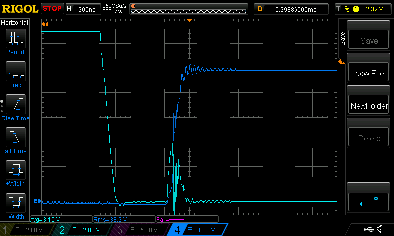 Here is the test setup, for the low side PNP turn off design. I used a BC557 PNP transistor. No idea if it's good enough for the test or not.  wronger than a phone book full of wrong phone numbers |
||||
| poida Guru Joined: 02/02/2017 Location: AustraliaPosts: 1389 |
further to the problem of negative gate voltages appearing at the gate drive IC output pins: This is a capture of the low side gate voltage (Light Blue) and the gate drive IC output (Purple) when using a Madness power board with it's totem pole transistor gate drive. 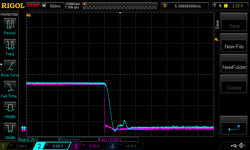 This is about the same position in the 1/2 wave output. what I see here is normal low side gate voltages, sometimes below zero, and always having some dv/dt or di/dt induced shoot through. But, and this is most important in my view, there is little or no negative voltages brought back to the gate drive IC output pins. This is a good result of the totem pole drive, which takes a signal but does not drive anything back along the signal path to the drive IC. I like very much the performance of Madness's power board. I think the very fast fall time of the gate drive IC output is due to it not having to drive a MOSFET. It drives instead the two base pins of the totem pole transistor circuit which probably has a quite low capacitance. We can then see the gate voltage (the output of the totem pole drive) follow a slower path due to the capacitive loading due to the MOSFET's gates and the transistor's switching speeds. Oh no. not again. I have made a mistake. I said earlier that these negative voltages see their way back to the drive IC output pins. No so. Here it is and it's no problem.  Purple is IC output pin voltage. Light Blue is low side gate voltage. Nope, no problem at all. It was a case of If I recall Incorrectly..... Edited 2019-10-19 19:58 by poida wronger than a phone book full of wrong phone numbers |
||||
| wiseguy Guru Joined: 21/06/2018 Location: AustraliaPosts: 1001 |
BC557 has a peak collector current of 200mA & continuous 100mA. I always use the PN2907A for this, continuous collector current of 800mA @ only 3cents ea from E14. They perform well in this application. Note E & C Pin out is different (transposed) New house build has taken over my life for now but handover is just a few weeks away. So no inverter playing for me for many weeks.  Putting opto-coupler drivers such as the TLP152 or FOD3180 on the FET power board in close proximity to the FETs and using Warps cross coupled opto drive method and using isolated gate driver power supplies for high and low side appears to have solved most of these issues for me. If at first you dont succeed, I suggest you avoid sky diving.... Cheers Mike |
||||
| Warpspeed Guru Joined: 09/08/2007 Location: AustraliaPosts: 4406 |
I am sure that a great many of these seemingly random catastropic blow ups are due firstly to noise and grounding issues, and secondly to chaotic startup and shutdown conditions where several different power supply rails are all changing relative to each other, below their final stable running voltages. None of this is likely to show up while monitoring a continuously running inverter. The "oh it went bang when I powered it up" can be quite misleading. It may have been fatally damaged in the final moments at the last power down when the microcontroller gave a final dying gasp at two volts dc supply, and succeeded in turning on both upper and lower mosfets simultaneously for an instant. What actually happens in any digital or software driven system as you slowly reduce the dc supply voltage down to zero ? Do gates and flip flops always continue to work in predictable ways ? An undervoltage reset on the microcontroller might work, or might not. So all the I/O lines on the microcontoller default to high impedance inputs at undervoltage reset. How would the gate drivers see that condition ? But what about the rest of the gate driver system as the supply voltages are all changing ? Its far from easy to sort all this out, but it absolutely must be thought right through. Cheers, �Tony. |
||||
| Solar Mike Guru Joined: 08/02/2015 Location: New ZealandPosts: 1125 |
Poida, try using a pnp with more current capability, you want to lower the impedance across the gate-source junction such that the gate voltage cannot increase. Keep the leads connecting to the mosfet really short eg 5mm. As it is the dv/dt rise time of the upper mosfet causing this, have you tried increasing the gate resistor slightly of that mosfet; this will slow it down a bit, lowering the rate of voltage rise on the lower mosfet drain. Try 10R, I assume you are currently using something less than that. The 220R and 104 monolithic cap snubber may not be the correct values for your setup, leave them off, measure the actual frequency of the oscillation and work out the correct values. Cheers Mike |
||||
| Warpspeed Guru Joined: 09/08/2007 Location: AustraliaPosts: 4406 |
The 2N2907A is probably a pretty good choice for this. Its fast with a fairly high current rating, but the gain is not that high, and gain is going to fall even further at full rated current. I still believe a high current mosfet driver such as the TC4452 would be a better choice than a bipolar transistor. Gate series resistor is a compromise between speed and excessive ringing. Layout is critical. Cheers, �Tony. |
||||
| Solar Mike Guru Joined: 08/02/2015 Location: New ZealandPosts: 1125 |
Agree, but difficult to retro-fit to an existing pcb, If a pnp soldered directly to the mosfet leads makes a noticeable improvement, then easier to get something working. Mike |
||||
renewableMark Guru Joined: 09/12/2017 Location: AustraliaPosts: 1678 |
Power Jacks came with a ferrite on the centre. If you are using those boards maybe re instate that and test. Cheers Caveman Mark Off grid eastern Melb |
||||
| poida Guru Joined: 02/02/2017 Location: AustraliaPosts: 1389 |
thanks all for your replies. I think I need to make a couple of tests now, 1 - use the 2N2907A and compare with none and the BC557 2 - design and source PCBs that use TLP152 with complimentary drive I think I already tried a ferrite bead, but I can do it again quickly. I like very much the bolt on MOSFET board design of the powerjack, it let's me try things very easily and cheaply and be able to compare one setup with another side by side. wronger than a phone book full of wrong phone numbers |
||||
| noneyabussiness Guru Joined: 31/07/2017 Location: AustraliaPosts: 506 |
https://www.microsemi.com/sites/default/files/micnotes/APT0402.pdf App note apt0402 Poida, another interesting app note on using ferrite beads.. particularly interesting is the info on using zener diode clamps can actually INCREASE the parasitic oscillation, doesn't mention TVS diodes, and i am aware they have a smaller capacitance than standard diodes purposely.. anyhoo, hope this helps... Edited 2019-10-29 11:53 by noneyabussiness I think it works !! |
||||
| djull Newbie Joined: 28/10/2019 Location: FrancePosts: 9 |
Hi everyone.  I read since some days your experiences about building inverters and it's amazing. Good work ! Then I have some questions I don't find myself a clear response. Regarding control boards, are they all compatible with remote ON /OFF switch (NOT push type) and some long cable to another device in order to cut off the inverter safely if needed as commercial inverters have. For lifepo4 it's a mandatory feature. Especially nano boards I read something about ON OFF push button so it won't work. Then I care about idle power, and Oz inverter power stage of control board to feed 12V and 5V seems not optimized at all here (series power resistor, big 2x heatsinks on mosfet) and I ask myself if this simple and maybe bulletproof design is done for some reasons instead of using something more efficient like 7812 and 7805 like in nanoboards. I found also some contradictory information about 12 or 18V supply here (OZinverters - with use of 12 or 18V zener diode). It's clear it was 12V initially but I don't know why push 18V now and if it's mandatory or not. Thanks a lot in advance. |
||||
| poida Guru Joined: 02/02/2017 Location: AustraliaPosts: 1389 |
Hi djull the Oz inverter has a continuous on/off control. The nanoverter has a momentary switch, normally open in the unmodified design. I am running a nanoverter based inverter at home with modifications which include a continuous on/off control. The inverter is commanded to run by pulling a pin down to ground. To stop it, let the pin float (pulled to 5V via on-board 1K resistor) I control the home inverter to make best use of the day's solar energy yield. Some days I get less than enough to run the inverter for 24 hours and so I have to stop the inverter at a low voltage set point to avoid battery damage. Then after more energy has recharged the battery enough, I restart the inverter. This requires a reliable on/off control and it works fine. The cabling is not shielded and in my installation there is no problem from EMI here is the code I am running on nano2: nano2_5_ac_current_sensor_continuous_on_off_control.zip I would not worry too much about the 5V and 12V supply design. Maybe 75mA @ 5V is needed to run the 2 nanos, sensors etc. I see about 0.8A @ 12V on my inverter when both fans are running. The 15V, used for the gate drive IC supply is not much either, maybe less than 100mA The above is not a lot of power and if you use genuine 7805 and 7812 regulators you will get good results and rated output (1A @ 12V). Avoid cheap regulators and fakes obtained from dubious suppliers. The 12V gate drive supply as used on the Oz boards is fine. No problems and no reason to think it could be improved with a higher or lower supply. The nanoverter uses 15V for the gate drive supply and that is good but to my mind not very much better or worse. It's just the voltage chosen by the board designer. It is nice to ensure the gate voltage is driven good and high, to ensure the lowest ON resistance. But the HY4008 has upper gate voltage limits so it's a good idea to keep it sensible. wronger than a phone book full of wrong phone numbers |
||||
| djull Newbie Joined: 28/10/2019 Location: FrancePosts: 9 |
Thanks a lot for this quick answer. I laughed when seing the line in the middle of your code  If I well understand, some designs started from Powerjack power boards some years ago which are not sell alone anymore. Today we found easily "cheap" power boards on all size from 8 to 24 HY4008 Fets with one small control board with EGS002 chip fitted on it. From my understanding, the weakness of these boards may be "real" power (heatsink a little bit small compared of mosfet numbers, some control weakness with over current protection which is better to deactivate (which components to remove ??) , small caps, etc... I think the small caps may not be too much a problem with lifepo4 and short and good sized cables but I may be wrong here :) Let's take some margin here and say a "4 kVA board is better to fit to a 3kVA core (maybe 2 kva only). It may be a good start to get a good and cheap inverter, as the main problem will be the transformer and the choke. Am I right ? I am asking myself if a nanoboard designed to put in place of this EGS002 board for better reliability is a do-able and a cost effective / interesting idea  |
||||
