
|
|
Forum Index : Electronics : Various aspects of home brew inverters
| Author | Message | ||||
| iannez Newbie Joined: 05/07/2019 Location: ItalyPosts: 23 |
Hello, I'm actually studying the DDS implementation like this: http://interface.khm.de/index.php/lab/interfaces-advanced/arduino-dds-sinewave-generator/ the signal comes out from pin11 or pin3 if it is enabled through TCCR2A registers and pinMode. I need it to study some behaviors of a sine wave, strictly at low voltage such as the output from a 50w class A/B amplifier, superimposed on another sine wave, but for this they must be in phase with PLL as on nanoverter sketch. thanks A. Cheers, Angelo |
||||
| poida Guru Joined: 02/02/2017 Location: AustraliaPosts: 1389 |
Here is the B-H curve of a IE transformer taken from a cheap UPS. I think it was 600VA and had 2 x 12V 7AH SLA batteries. You get about 15 minutes run time when you have a typical low spec office PC and LCD monitor as the load. This is at 50Hz: 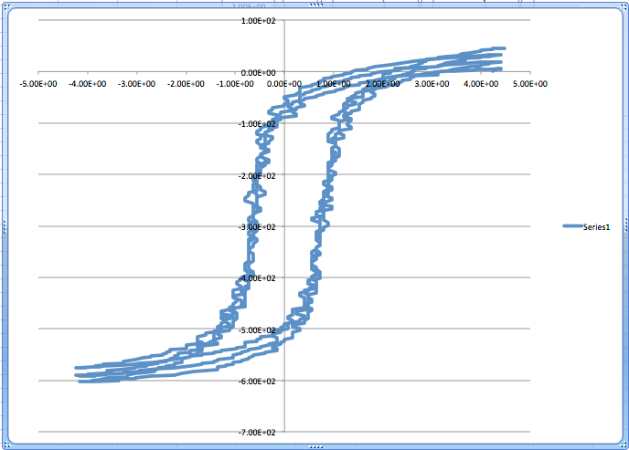 This is a lot of saturation. No wonder the UPS is cheap to buy. And the battery powered run times are poor. wronger than a phone book full of wrong phone numbers |
||||
| poida Guru Joined: 02/02/2017 Location: AustraliaPosts: 1389 |
Hi Angelo This is how nano1_7_etc type code works: a 20KHz timer with PWM is set up. Each time the timer calls it's interrupt some work is done. For the inverter application, we need a PWM pulse train on one pin (D9) and the other pin (D10) is held LOW. This is maintained for 1/2 of the 50 Hz cycle. Then for the other 1/2, D9 and D10 functions are swapped. We are driving 2 half bridge inverter output stages. The PWM pulse train is taken from a lookup table of precomputed values of a 1/2 cycle sine wave. I wonder what your project entails. I guess you are studying this at school or university. I think you would like one pin only to output PWM pulse widths that range from near 0% to near 100%. This implies "zero AC volts" would be 50% width exactly. Now you will have a DC offset of about 1/2. This can be removed with AC coupling. here you go: nano_1_v7_no_bessel_angelo.ino.zip Here is D9, low pass filtered with 4.7K R and 220nF cap, Light Blue Yellow is D7, the 50Hz heartbeat or CRO trigger Note the vertical scale and zero position for D9. It is DC coupled. 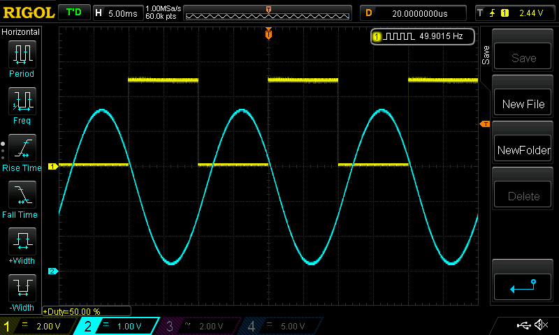 wronger than a phone book full of wrong phone numbers |
||||
| iannez Newbie Joined: 05/07/2019 Location: ItalyPosts: 23 |
Hello Podia, thanks for the edited sketch! I almost understood how everything works ... I am over 40 and I don't go to university, even if that's one thing in the lineup that I would like to do sooner or later. I consider myself an experimental physicist in heart and mind, first because I love physics and then because I adopt this type of philosophy also in life, but in my daily work I am a humble linux system administrator. I have always had a passion for electronics. but unfortunately I discovered microcontrollers only this last year due to Covid as I am working from home and I have some time to devote myself to these studies. I tested your sketch and obviously it works perfectly: D as a generator I used the sketch present at the link on the previous page which uses the dds technique and produces a very stable sinusoid in frequency, also modifiable via pot if desired. some photos: phase KO, no pin D2 linked 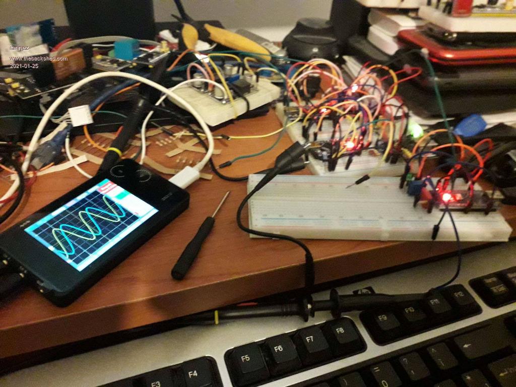  phase OK, pin D2 linked via optocoupler and green LED light  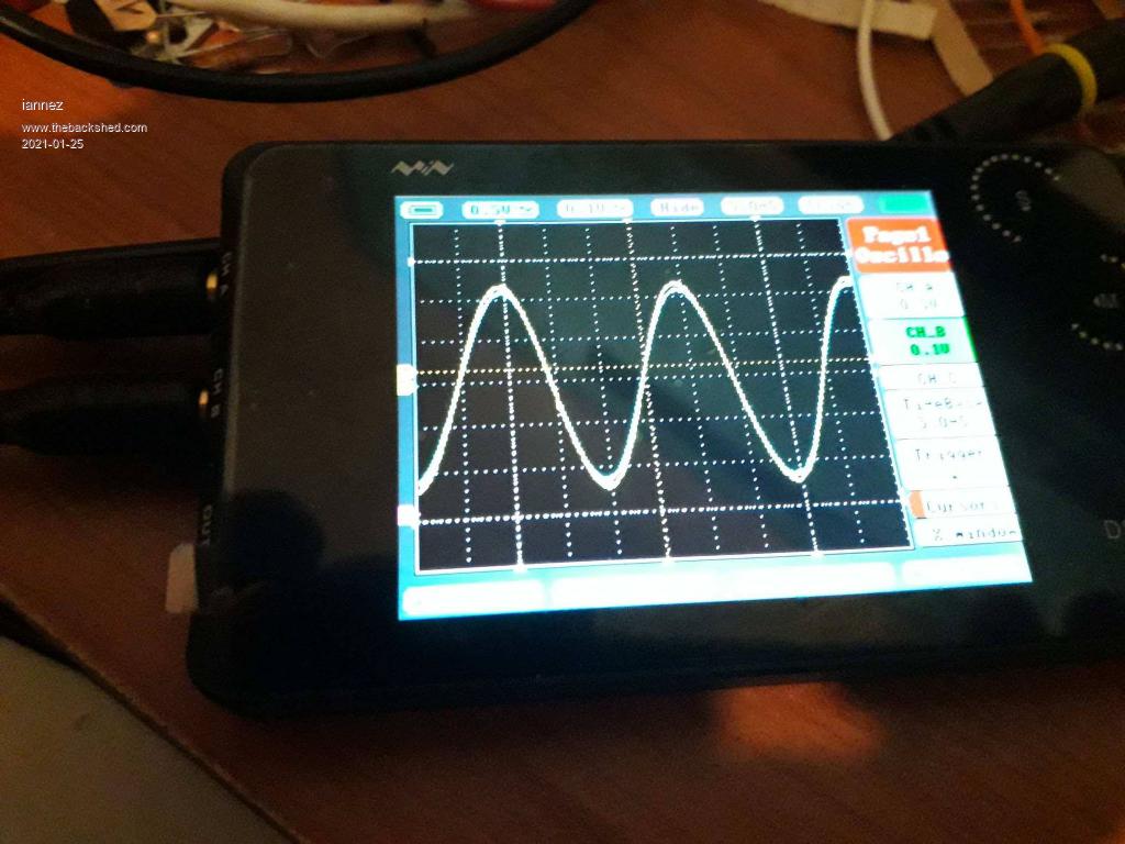 in the last photo there are the two superimposed waves I apologize for the awful setup. I will buy a rigol 1054 as soon as possible :) I only had to "modify" a couple of things to get the two waves in perfect phase with the same zerocross. I read about this practice in one of your previous posts. I inserted the _pcorrect variable which is managed through pin A0 mapped in the boundary values -200, 200 because I did not know regardless the correct value. I did some tests :) then I made the variable fixed so it doesn't flicker in real use. volatile int _pcorrect; void loop() _pcorrect = map(analogRead(A0), 0, 1023, -200, 200); //_pcorrect = -169; ISR (INT0_vect) phase_error = (pcint - _pcorrect); //default value sketch orig. 4 I guess there is an automatic way to make the phase shift tend to about 0. in practice now it is like the nano variac but with PLL and fullwave, great for experimenting with a couple of things without using the H bridge and using low voltage for now :) I hope I can ask you a few more questions about the operation of the sketch without abusing your patience. I have already read all the threads concerning the nanoverter, but I can't find the correlations in the use of some variables. #define NPWM 200 here it is clear, number of sinusoid points created in array l, even if you then create one with 201 points. #define PPWM 800 here I imagine that 800 derives from dividing the arduino clock (16mhz) by 20khz of the PWM carrier 16 000 000/20 000 = 800 correct? but when you use it here OCR1A = PPWM / 2 + c; what does it mean? uint16_t l [NPWM + 1]; why do you use 200 + 1 values? to something to do with the v1low toggle? to get 50hz we use 20khz / 400 = 50hz if I use 201 I get 20khz / 402 = 49,7512hz what logic should i follow? I probably lost something on the way :) thanks for your time, A. Edited 2021-01-25 01:33 by iannez Cheers, Angelo |
||||
| poida Guru Joined: 02/02/2017 Location: AustraliaPosts: 1389 |
Angelo: it's good to see you having a play with this code. I was wrong with my guess you were a student! sorry. (I also do linux IT system admin.) PPWM is the time, in clocks for a 20KHz PWM, and so it is put into ICR1. 200 of these 20KHz pulses is 1/100 second, so we can make one half of the 50 Hz sine wave using the 200 PWM duty width values. The Nano (and a lot of other microcontrollers) use tiny crystals for the clock, and they can be quite stable but not so accurate. The nano I tested your code on gives 49.900 Hz with PPWM = 800 Using 798 it is now 50.027 Hz Feel free to change this to obtain a closer output to 50Hz. Note that this was done without any signal on D2, potentially altering the output via the phase lock loop OCR1A = PPWM / 2 + c; In your version of the firmware, we need to use one pin only for PWM output. Sine wave is bipolar. It ranges between positive and negative values. I can't output a negative voltage via a pin. So I offset the sine wave 1/2 it's amplitude to permit it to vary between 0 and 5V so it needs to be offset by 2.5V PWM duty width ranges from 0 to PPWM (in clocks) To make 2.5V use a duty width of 800/2 or 400 clocks. So I always output a duty width of 400 plus or minus the sine wave modulation which will vary +/- 400 clocks or a little smaller for safely avoiding under or over flow. why do you use 200 + 1 values? Just in case I make a mistake in code and go "out by one" in my counting or addressing. This does not happen with the code now since it's so mature and so we can remove this to save 2 bytes of RAM. Always use NPWM = 200 The phase lock code is an unprofessional solution to synchronising a signal with an input. But it works. The end result of the code is to add or subtract one extra PWM output for the nominal 50 Hz output frequency, to make the output track the input pulse on D2. This is the smallest change I can make to the output but it contributes to a lot of phase noise. I do fractional math to carry 10 bits of precision in the PLL error term. The performance of this PLL is not bad, it always locks when given an input within about 50Hz +/- 1Hz. It can maintain lock +/- 2 Hz when I test it. wronger than a phone book full of wrong phone numbers |
||||
| poida Guru Joined: 02/02/2017 Location: AustraliaPosts: 1389 |
I just made a big change to the sync code where instead of adding +/- 1 extra pwm pulse to the output, I am now adding +/- 1 clock to the 20kHz PWM pulse generator. This means finer control over the output waveform. The width of the Dark Blue trace is the tracking error. Before: 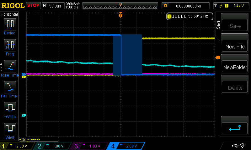 After: 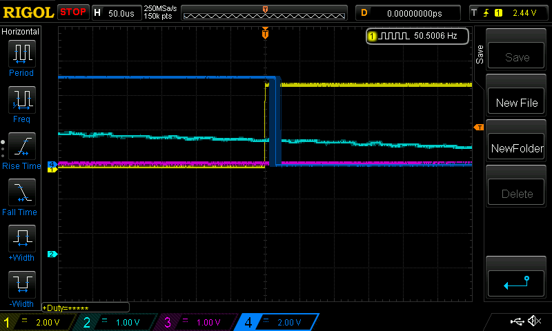 It's about 5x better. here is the improved PLL code: nano_1_v7_no_bessel_angelo_syncv2.ino.zip Again I use fractional math to calculate a running trim factor to the main PWM pulse gen frequency. The tracking error is about 20us for a 50Hz frequency so it's 20uS / 20mS x 360 = 1/1000 * 360 or 0.36 degrees wide It's +/- 0.18 degrees tracking error! Edited 2021-01-25 13:43 by poida wronger than a phone book full of wrong phone numbers |
||||
| iannez Newbie Joined: 05/07/2019 Location: ItalyPosts: 23 |
Good evening everyone and hello podia! I tried the new sketch, it's perfect! the wave is tracked perfectly, in a short time I will do the test of the two superimposed voltages with connected light load. I have inserted these lines in the sketch which probably improve the overall system noise. with my instruments I do not appreciate the differences, maybe with your rigol1054 you notice something. #include <avr/power.h> setup() { //https://www.gammon.com.au/forum/?id=11497 //power_adc_disable(); // ADC converter power_spi_disable(); // SPI //power_usart0_disable();// Serial (USART) power_timer0_disable();// Timer 0 //power_timer1_disable();// Timer 1 power_timer2_disable();// Timer 2 power_twi_disable(); // TWI (I2C) DIDR0 = DIDR0 | B00111111; //Digital input disabled on all ADC 0-5 ports } let me know otherwise if there are no differences I delete them: D to see if I understand how the new sketch works I will try to experiment on a sketch with different PWM freq and NPWM in order to verify how the parameters affect. thank you soon, A. Cheers, Angelo |
||||
| iannez Newbie Joined: 05/07/2019 Location: ItalyPosts: 23 |
I added another control led sync on pin 11 for synchronism check, visually. every so often a blink comes out a led though remains in sync, probable threshold to be adjusted. if (abs (phase_error) <3 && abs (new_delta) <80) A. Cheers, Angelo |
||||
| poida Guru Joined: 02/02/2017 Location: AustraliaPosts: 1389 |
NO difference. wronger than a phone book full of wrong phone numbers |
||||
| iannez Newbie Joined: 05/07/2019 Location: ItalyPosts: 23 |
Good evening everyone, thanks podia for the test, I immediately deleted those lines. there was a test, sometimes a trivial line changes everything I am continuously in test :D I did some tests NPWM at 400 and PPWM 399 as per eq. of the manual for timer1 mode14: ICR1 = (F_CPU / ( timer1Prescaler * DesideredFreq )) - 1; the wave is good but it is more stable in the eye with prev values. perhaps the RC filter should be reviewed or probably micro at the limit. also the memory is obviously almost full, just a test. i am waiting for two power supply to power the test bench I plan to do. maybe a friend offers a 4channel oscilloscope so in the new line: ICR1 = PPWM - (pcount_delta / 256); now it is clear to me that from the ICR1 which regulates frequency, subtract a part of the out of phase that was calculated in INT0, so as to follow the wave for the sync minimizing the phase difference. but where does 256 come from? and also: new_delta = 8 * (phase_error / 2 + 8 * (phase_error - old_phase_error)); in the comment I read PID but obviously the logic behind it is foreign to me thanks for the clarifications and good evening, A. Edited 2021-01-27 02:39 by iannez Cheers, Angelo |
||||
| iannez Newbie Joined: 05/07/2019 Location: ItalyPosts: 23 |
I also post this video of a guy I was following long ago. he had implemented a core saturation protection of transformers so as to save the H bridge in the event of a short because of the saturated core => short. poida, it could be useful in the study of a few posts ago. https://www.youtube.com/watch?v=3LkpzQ_LuJ0 bye A. Cheers, Angelo |
||||
| poida Guru Joined: 02/02/2017 Location: AustraliaPosts: 1389 |
Angelo: I see you experimented with 2x PWM frequency which becomes 40kHz. It can help some things such as reduce inductor saturation but it means also 2x switching losses. In our inverter builds switching losses are not very large to begin with so you and I have scope to experiment. In the PLL code, which executes once each falling input zero crossing of the 50Hz input, some calculations are made. First I get a phase error. I also get the change in phase error from the prior interrupt. Next I obtain a correction factor, to be applied to the timer counter of the 20kHz timer. The correction trims the normally 800 by a small amount to alter the 20kHz by a small amount, up or down. The trim factor is new_delta = 8 * (phase_error / 2 + 8 * (phase_error - old_phase_error)); I could simplify this expression but it allows me to easily try changes to the expression. It takes 4 x phase error and 64 x phase error change and this result is accumulated (or subtracted) into a running total called pcount_delta This is going to be large number and it will continue to grow larger or smaller while the PLL is not locked. pcount_delta is divided by 256, which can be executed fast without a divide instruction and THIS result is subtracted from the base value of the 20kHz timer count of 800 to yield the new timer count. The divide by 256 is used to maintain 8 bits of remainder in the division to carry over better accuracy in the system. It's just factional math and it's fast. PLL background: some PLL designs multiply the lock signal by the system output signal. You get a cosine (sine x sine = cosine) and then take all but the DC from it and use the DC to steer the local oscillator into phase lock via a feedback mechanism. This PLL obtains the phase error directly and infers the two terms needed for feedback to work (phase and frequency). I produce a feedback correction term from something like 4 x phase error + 64 x frequency where the units are 8 Mhz clock counts. The control loop is a simple first order PID. The proportional component is phase error The differential component is frequency There is no integral term. I can not discuss the PLL workings any more since I lack the mathematical background required (loop stability, Bode plots, S transforms, etc.) wronger than a phone book full of wrong phone numbers |
||||
| iannez Newbie Joined: 05/07/2019 Location: ItalyPosts: 23 |
Goodmorning everyone! thanks Poida for illustrating the logic you constantly implement. you use the powers of two as truncators to then keep the 8bit in the calculations. as a bitshift >> 8 (2 ^ 8) which the cpu interprets quickly. and the PID as a filter of a certain order via software. i like this type of mod, something slowly I understand I actually experienced the possibility of increasing the number of NPWM p oints to give a better shape to the output wave (not that at 20khz it is bad!) unfortunately I don't have a distortion meter or a better oscilloscope that allows me to visually check. the rise in frequency is the consequence. I calculated a whole series of useful frequencies that gave out integers that can be used. there may be problems with the PLL but that's another story PPWM: 200 | FREQ: 80000 | NPWM: 800 PPWM: 250 | FREQ: 64000 | NPWM: 640 PPWM: 256 | FREQ: 62500 | NPWM: 625 PPWM: 320 | FREQ: 50000 | NPWM: 500 PPWM: 400 | FREQ: 40000 | NPWM: 400 PPWM: 500 | FREQ: 32000 | NPWM: 320 PPWM: 625 | FREQ: 25600 | NPWM: 256 PPWM: 640 | FREQ: 25000 | NPWM: 250 PPWM: 800 | FREQ: 20000 | NPWM: 200 PPWM: 1000 | FREQ: 16000 | NPWM: 160 PPWM: 1203 | FREQ: 13300 | NPWM: 133 PPWM: 1250 | FREQ: 12800 | NPWM: 128 PPWM: 1280 | FREQ: 12500 | NPWM: 125 PPWM: 1600 | FREQ: 10000 | NPWM: 100 PPWM: 2000 | FREQ: 8000 | NPWM: 80 i found the limits using timer1 mode14 with values PPWM: 200 | FREQ: 80000 | NPWM: 800 because it goes beyond the memory ability, that would be 1600 per fullwave. I haven't tried with the PROGMEM but I think the limit is the same. and below PPWM: 1000 | FREQ: 16000 | NPWM: 160 it might not make sense because the frequency would become audible on an H-bridge and the number of NPWM points would be too low in my opinion. I remember that my application is for now different from the inverter one. I say for now why the Chinese inveter taken on aliexpress must arrive: D now i just need to have a super imposed sine wave in phase and with the same zerocross. adjusting amplitude should decrease the overall output voltage or increase it. almost like putting two secondaries of a transformer in series. Transformer AVRs work like this through relays that switch on various secondaries. so... I took a while to understand how I could reset the distance between the two zerocross of the waves. so automatically have superimposed wave with concident zero cross, without using the _pcorrect variable that I introduced and which refers to the analog pin. i thought if i used another ISR interrupt (INT1_vect) on pin3 on which then to enter with our filtered rc wave (of course a square would be better but it should go anyway) in the ISR I could calculate an additional pcint. ISR (INT1_vect) { pcint1 = pcount + (v1low == 1? NPWM: 0) - NPWM; // get position in 50Hz waveform, -200 to 200 counts // pcint is position in output waveform when this interrupt occurs } the difference between the two pcint of the two ISRs should give the distance in pcount between the two zerocross. _pcorrect = pcint1 - pcint; if the logic is correct you put this value in the final calculation of the phase_error. what do you think about it? thank you soon, A. Edited 2021-01-27 21:43 by iannez Cheers, Angelo |
||||
| poida Guru Joined: 02/02/2017 Location: AustraliaPosts: 1389 |
Angelo: feel free to alter the code and try out ideas. I think it's a fun way to discover and learn. nano_1_v7_no_bessel_angelo_syncv5.ino.zip is the result of a couple of days play. I found I could tune the 50Hz by altering the 20kHz timer, adding or removing one of the 800 clocks from the timer count. I now do this in a more sophisticated manner: for the entire 50Hz cycle, I modify the 800 clock count adding or subtracting a clock (or not) to give the required trim. Again I need a bit of fractional integer math. The guts of the change: i = pcount_delta/256; ICR1 = PPWM - i; pcount_delta = (pcount_delta - 256 * i) + pcount_acc + 135; // 135 is trim for the 16MHz clock is not quite 16.0000MHz // the trim puts the PLL loop correction at zero with a 50.0000Hz input signal. // other wise pcount_acc would = 135 plus any calculated trim. which occurs at the start of the 20kHz timer 1 overflow interrupt. The PLL loop produces a value "pcount_acc" and this will increase or decrease the frequency of the nominal 50Hz. If this = 0, then no change. pcount_delta just accumulates the trim, and I get the top 8 bits, subtract it from the 800 clocks, then calculate and leave the low 8 bits in it ready for the next increment of pcount_acc. This all permits me to carry 8 bits of accuracy after I do the integer division. Results are good. When the PLL is fed a fixed 50Hz to track from the signal generator the original code is: + 50.0039 Hz - 49.9988 Hz with a 100uS wide uncertainty of lock position. The above code gives: + 50.0014 + 50.0003 and 20uS uncertainty The frequencies are as reported by the DSO on the PLL locked 50 Hz output. It's input was always 50.0000Hz wronger than a phone book full of wrong phone numbers |
||||
| iannez Newbie Joined: 05/07/2019 Location: ItalyPosts: 23 |
Goodmorning everyone! Podia great job as always. very hacker mode :) done some tests and with my miniDSO the waves are superimposed with perfect tracking, i am saving to buy a serious DSO that allows me to appreciate any changes or software tests. it is impossible for me to measure in this way. I just changed the interrupt mode for testing // EICRA = 3; // interrupt on falling edge from pin D2 EICRA = 2; in order to have the coinciding zerocross because in my case the waves were out of phase but in lock. the same thing can be done manually using the variable _pcorrect in the ISR as I did before, but now it's not needed if the interrupt catches the wave in the right rising / falling edge. phase_error = (32 * (pcount - 32 + (v1low == 1? 200: 0) - 200 - _pcorrect) + pe_frac); I believe we can do better if one wants to use this mode, if necessary. the way you use the terms of the PID is great! I have to practice using the PID because it is essential. I did the double interrupt test INT0 and INT1 and it works but it is slower and less precise, it probably makes sense only if the phase tracking is not as good as the one used here, so everything is simpler and faster ... I have a rigol ds1022 "waveform generator" with here I do some tests, but if I use direct the output inside the pin D2 of arduino nano, the waveform is distorted ... what can you advise me to avoid this problem? should i use some buffer opamp before entering direct? the ds1022 has the ability to phase out the wave so as to verify the various locking modes of the PLL interrupts. one of the packages from aliexpress has arrived but not that with inveter inside, we wait :) psu will also arrive this week for the tests of this sketch, i hope thanks always for your time, bye, A. Cheers, Angelo |
||||
| poida Guru Joined: 02/02/2017 Location: AustraliaPosts: 1389 |
The DG1022 is a good generator. Default output is bipolar. You can set output to have a DC offset. So, choose 2.5V DC offset with wave amplitude of 5V. Output will now range from 0 to 5V. The distortion you are seeing is probably due to the negative part of the waveform output from the DG1022 being clamped to near zero thanks to the nano digital pin internal diode protections. wronger than a phone book full of wrong phone numbers |
||||
| iannez Newbie Joined: 05/07/2019 Location: ItalyPosts: 23 |
thanks Poida, it actually worked! bye, A. Cheers, Angelo |
||||
| iannez Newbie Joined: 05/07/2019 Location: ItalyPosts: 23 |
Goodmorning everyone! 3 kinds of inverter arrived from aliexpress so i can also experiment. the first, simple squarer that drives driversfinals: 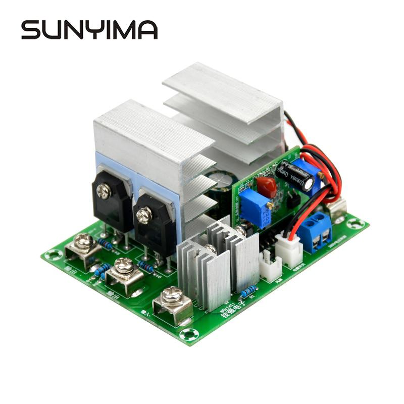 the second, EG8010 which drives power amplifiers + recycled ups transformer.  the third, AC/DC converter with SG3525 and EG8010 for direct DC/AC on H-bridge with high voltage. 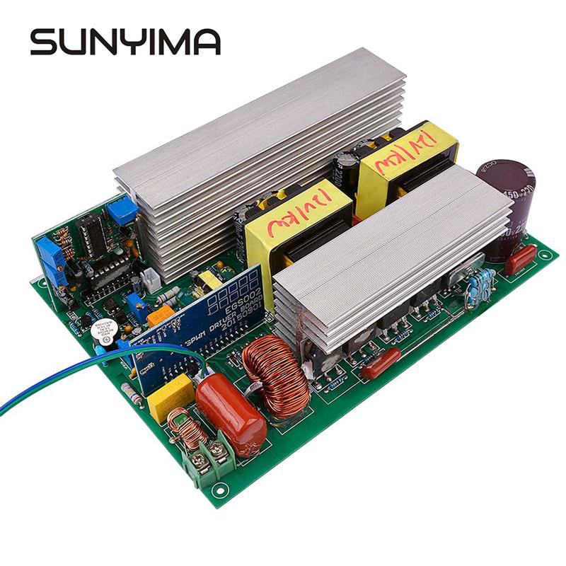 with great amazement all 3 inverters work, proved simple a few watt incandescent bulb + current limiter DC input for safety, you never know. life expectancy at 80% of power output is a mystery. I have a couple of questions regarding the last two inverters to which I cannot technically answer. - we have a way / circuit to bypass EG8010 and use Chinese low voltage hardware with arduino and sketch nano1? I assume you need drivers like the ir2110 or similar present on the EG8010 and something that emulates the protections offered by the opamps. I would like to be able to test the sketch with as little hardware as possible on Chinese inverter. - why is the high voltage inverter not used in the amateur field? my first answer is to be sure not to handle DC at 310 or more volts. I assume that the sketch nano1 can safely drive through drivers with adequate dead time, a high voltage H bridge. if safety and efficiency are not the problem, what would improve using the output transformer? - is there a way to deform inverter output waveform in a controlled way? i know series diode test on light bulb to saw waveform, as did Peter in this thread pages ago. but it would be useful to introduce other types of distortion such as the inductive type that is generated by a fridge motor or a starting drill. but without using a fridge or a drill that consume too much current. an LCR circuit that distorts in the same way but with low consumption? I apologize in advance for the probably trivial questions for some people. i am trying to figure out how to correct the inverter output shape. this without relying only on the voltage peak dictated by the feedback to follow the output voltage on both half-waves (I imagine a half-wave on unipolar EG8010) the idea is to sample the output waveform and compare each sample to the one present in array l[NPWM] at the same time of reading. the difference between the comparison gives the value to be given in the OCR1A when it will create the output PWM pulse to correct the output deformation. can my logic be correct? adding a few lines to the sketch I calculated the time it takes the ISRs and ADCs to do their thing, as Peter had already written in the comments. if the ADC readings are few and accurate, thanks to internal VREF from 1.1, I think the waveform control idea is feasible. I also ported the sketch to stm32f103c8 (blue pill) without using stm32duino but STM32 on IDE arduino. bare metal registers are crazy, but once you understand everything works perfectly. ln attached if anyone wants to experiment. there are not all active pins but only those for testing which I played on breadboard. obviously you can then import them if necessary. 2021-02-11_154623_stm32f103c_nano_1_v7_no_bessel_angelo_syncv5_forum.zip I tried the port to understand how much the timing affects etc. but it is how the code is written and the use of registers that make the difference, always. I will also try to use the stm32f411 (blackpill 100mhz) but I assume there are no problems whatsoever o improvements apart from points per wave and pwm frequency tested only on breadboard for now. thanks for your advice on my doubts, Ciao! A. Edited 2021-02-12 01:16 by iannez Cheers, Angelo |
||||
| poida Guru Joined: 02/02/2017 Location: AustraliaPosts: 1389 |
Hi Angelo I've just got back from work where I had to make a $100,000 AU machine work after one of it's 2 CPU Z80 based control boards died. Or die trying. This most recent post is about 15 times more complex than I can deal with right now. My first thoughts are that you can substitute the EG8010 control modules with a nanoverter. Just make a cable that takes the 10 pin IDC socket and goes to the 15 pin or whatever 0.1 inch header. It's all electrically compatible. So that is one experiment: compare and contrast the EG8010 and the nanoverter. I will help with how you do this, I think it's worthwhile. But maybe tomorrow I will read the above and hopefully bring some extra value to the conversation. wronger than a phone book full of wrong phone numbers |
||||
| iannez Newbie Joined: 05/07/2019 Location: ItalyPosts: 23 |
Hello Peter, Z80 distant memories of youth! my first"PC", a Toshiba MSX I was 9 years old, gift for communion. first steps with basic language, the internet was still in Tim Berners-Lee's head that I give it to the world a year later, in 1989. Federico Faggin the father also of the Z80, excellent physicist and superb engineer, I follow a lot on youtube in his conferences where he talks about his creations among others companies that he founded and not. really good times ... good rest, A. Cheers, Angelo |
||||
