
|
|
Forum Index : Electronics : Experimental sinewave inverter designs
| Page 1 of 7 |
|||||
| Author | Message | ||||
| Warpspeed Guru Joined: 09/08/2007 Location: AustraliaPosts: 4406 |
There appears to be a great deal of interest in writing software for a home brew PWM inverter, as well as looking at some rather different hardware approaches to inverter design. Its a fascinating subject and quite a personal challenge. My own software skills are rather limited, but I have managed to get quite a few rather unusual inverters working very successfully over the years, and have really enjoyed the challenge. I decided to start yet another inverter thread, but this one I hope should be rather different. Its for people with wider interests than just buying a Chinese PWM chip, or ready made PWM driver board. It follows on from the post I made on another thread. [quote] Generating a PWM sine wave directly from a lookup table is fairly straightforward. What makes it much more complicated is continuously adjusting (regulating) the output voltage, and in some cases programming the output frequency up and down as well. Its not difficult in theory to adjust the amplitude up and down, its just simple multiplication. The real difficulty is getting conventional software to do it fast enough in real time with fine enough time resolution for high frequency PWM. The way I have done this myself long ago, was to use a dual port ram. A basic microcontroller can do all the required number crunching, working as fast as it can, and continuously modifies and updates a sine wave stored in a dual port ram, which is then used as a lookup table template for one complete mains cycle. The bits stored in the ram can then be read out at a much higher speed from the second "output" port of the ram. This can produce high frequency PWM directly, using just a continuously clocked counter and a magnitude comparator. The counter clocking speed and ram "output" addressing, could be made variable to give a varying output sine wave frequency if that is a requirement. The dual port ram effectively isolates the software side from the much faster hardware driven output side. The microcontroller can chug along relatively slowly and continuously update the amplitude of the stored sine wave byte by byte completely asynchronously, and it can do that without any timing constraints. All sorts of goodies like PID control, and soft start can then readily be written into the software without disrupting the PWM output. The EG chip is probably some kind of common commercial FPGA chip that works in a similar way to the above, in that the various internal functions are pipelined, with several things happening simultaneously and at different speeds. Its the only way that I can see to get both the high speed and the very fine time resolution and include quite a few nice features all in a single low cost chip.[/quote] That approach has been my best shot so far in building a home made PWM sine wave driver board. But I have also used a similar approach to develop a multistep sine wave inverter that does not use high frequency PWM. Anyhow the main interest here seems to be only in high frequency PWM, and the software to achieve that. And there are many people here vastly more talented in software black magic than myself. So let's start the discussion and share a few ideas. Cheers, ĀTony. |
||||
| RFburns Regular Member Joined: 21/07/2017 Location: AustraliaPosts: 43 |
I watch with interest ;as I am software challenged (could read that as "an idea's man" - no Fk'n idea). However I have seen some working examples of inverter software written on the stm32f (an ARM processor) cheap an good performance STM32 cost this thing is good value and from the DATA Sheet - 20 KB of ram, sufficient to work with vectors and matrices; - 12 bit ADC with conversion time of 1 uS !!! This thing is fantastic! - The 75 MHz frequency allows the approach to algorithms where processing time is important; - 7 internal timers allow you to manage every situation; - 32-bit CPU means, probably, that it has no problem working with floating-point numbers Anyway good luck. About all I can contribute .RF Strong like horse smart like tractor! |
||||
| Warpspeed Guru Joined: 09/08/2007 Location: AustraliaPosts: 4406 |
A fast high end microcontroller would certainly help a lot, but its still going to suffer from the basic limitation that it can only be performing one task at any instant in time. If you run two processors, or one processor plus some external hardware, one processor can just be repetitively making the sine waves, and the other doing the housekeeping and performing supervision and various control functions. Neither should have to work terribly hard to be able to do that. Cheers, ĀTony. |
||||
| noneyabussiness Guru Joined: 31/07/2017 Location: AustraliaPosts: 527 |
Warp, what about a micro " creating " the spwm and a analog device ( external ) to adjust the peak/average of the waveform for voltage regulation? ? Sort of what you do with a square wave fed into a comparator and adjust the trigger point voltage ( feedback ) I think it works !! |
||||
| Warpspeed Guru Joined: 09/08/2007 Location: AustraliaPosts: 4406 |
Here is my most recent idea for the simplest possible hardware only pure sinewave PWM generator. 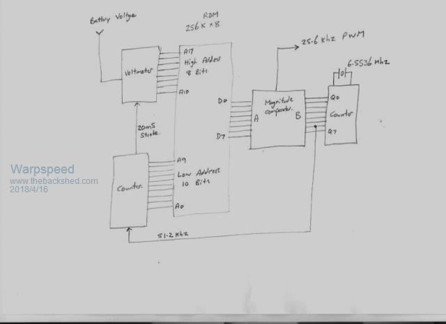 The idea here is that we use a very large ROM to store multiple 1K lookup tables. Each lookup table cycles through 1K fifty times per second using a 51.2 Khz clock. The data output of the ROM is compared to a high frequency counter to produce 25.4 Khz PWM with an 0-100% duty cycle. A digital voltmeter reads the dc battery voltage coming into the inverter, and selects a suitable lookup table to keep the amplitude of the PWM going into the transformer primary constant, regardless of any changes in battery voltage. Just as an example, we could easily cover a 2:1 input voltage by only using the upper half of the ROM addresses (giving 128 different lookup tables). The voltmeter would measure the incoming dc voltage once only at each zero crossing to select an appropriate lookup table for the next mains cycle. This has both advantages and disadvantages. The advantages are extreme speed of response, with total stability. Under very heavy loads the transformer output voltage is going to fall slightly, but hopefully not by enough to be a problem. The main challenge an inverter faces are large voltage changes at the dc input created at the battery. Many improvements are possible such as adding slow integral output voltage correction, or using more of the available ROM. But the aim here was to come up with something really simple using the fewest possible parts. Cheers, ĀTony. |
||||
| Warpspeed Guru Joined: 09/08/2007 Location: AustraliaPosts: 4406 |
What you are suggesting sounds very much like a high power class D switching amplifier. That is also a very interesting approach. Its basically a multi kilowatt PWM audio switching amplifier running with a 50Hz tone. The waveform purity would be excellent, and so would the output voltage regulation. 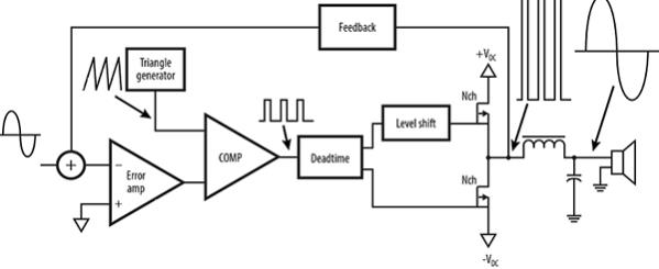 Cheers, ĀTony. |
||||
| noneyabussiness Guru Joined: 31/07/2017 Location: AustraliaPosts: 527 |
Exactly what I was thinking. .. d class amps are common and filtering etc. Is well established and well documented. Its just the unknown load, whereas speakers you can calculate easily (ish). I think it works !! |
||||
| noneyabussiness Guru Joined: 31/07/2017 Location: AustraliaPosts: 527 |
Class D avr Something along these lines, fed a 50hz sine wave I think it works !! |
||||
| poida Guru Joined: 02/02/2017 Location: AustraliaPosts: 1480 |
This might be fun. I have a prototype inverter designed to permit examination of the effects of a few variables such as 1/2 bridge gate drive dead time, PWM frequency, closed loop control methods and such. I have posted results here in the past. I have a basic inverter board built with 4 x IRF3808 which runs using either my prototype controller board or a EG002. I can swap either in 10 seconds and examine the results of the test. The system I have is using an Atmel Atmega 328 microcontroller (Arduidno Uno to be precise) feeding two gate drive signals and one output enable signal into 2 x IR21844 1/2 bridge gate driver ICs. I use an isolated 12V supply for the IR21844s. The IR 21844 takes a single input and generates the two complimentary gate drives for a 1/2 bridge. They also, via a resistor, let you set the dead time. They have an output enable pin which I use to important effect. I want to share the current code I am running. setup() is run once and initialises the sine wave table, variables and sets up the two timers that periodically run their particular code blocks. loop() is run repeatedly ad infinitum. #define cbi(sfr, bit) (_SFR_BYTE(sfr) &= ~_BV(bit)) #define sbi(sfr, bit) (_SFR_BYTE(sfr) |= _BV(bit)) #define NPWM 200 #define PPWM (160000 / NPWM) uint8_t f50,oen; uint16_t pcount,uf; uint32_t vpwr,sst; uint16_t l[NPWM+1]; float pwr,ch2,ch0; uint16_t dbounce; double Input, Output, Setpoint; double errSum, lastErr,error,dErr; double kp, ki, kd; float xv[10],yv[10]; void setup() { int i; float t,u; for(t=0.0,i=0; i <= NPWM; i++,t += 3.14159/ (float) NPWM) { u = 16384.0 * sin(t); l = (int)u; } pinMode(9, OUTPUT); pinMode(8,INPUT_PULLUP); DDRD = 0xff; // can NOT let arduino system alter any pins from D0 to D7 via calls to pinMode() etc.. It buggers d5 which I need to pull down low-Z upon boot noInterrupts(); TCCR2A = 0; // I had some bits set which interfered with simple digital in PORTD. set to zero means no i/o pins driven by timer2. TCCR2B = _BV(CS22)| _BV(CS21) | _BV(CS20); TIMSK2 |= (1 << TOIE2); TCCR1A = _BV(COM1A1) | _BV(COM1B0) | _BV(COM1B1) | _BV(WGM11); TCCR1B = _BV(WGM13) | _BV(WGM12) | _BV(CS10); OCR1A = 10; ICR1 = PPWM; TIMSK1 |= (1 << TOIE1); sst = 0; f50 = 0; pcount = 0; uf = 0; ch2 = ch0 = 0.0; pwr = 0.0; vpwr= 0; dbounce = 0; oen = 0; // set up PID 0.1 0.0 0.01 for biquad LP Fc = 0.02, np=4 kp = 0.1; ki = 0.0; kd = 0.01; errSum = 0.0; interrupts(); // enable all interrupts TIMSK0 = 0; // except arduino clock sbi(ADCSRA,ADPS2) ; // ADC clock prescale = 16 now. this saves 100us in main loop with little cost to loop stability cbi(ADCSRA,ADPS1) ; cbi(ADCSRA,ADPS0) ; } ISR(TIMER2_OVF_vect) {// 100 Hz TCNT2=100; pcount=0; f50 = !f50; TCNT1=0; uf=1; if(oen == 1) sbi(PORTD,5); else cbi(PORTD,5); check_switch(); } ISR(TIMER1_OVF_vect) {//20Khz SPWM long c; if(pcount == 1) // order of events is important. This gives the least time difference from 50Hz and 20kHz gate drive { // When this difference is big, larger AC output waveform distortion occurs. if (f50 == 1) cbi(PORTD,7); else sbi(PORTD,7); } c = (l[pcount] * vpwr) >> 14; // scale sin wave by vpwr 32 bit integer calcs. if (f50 == 1) // one 1/2 wave or other of 50Hz output OCR1A = c; else OCR1A = PPWM - c; pcount++; } void do_pid() { double timeChange = 0.01; // always called at 100Hz, so dT will be 10msec.. error = Setpoint - Input; errSum += (error * timeChange); dErr = (error - lastErr) / timeChange; Output = kp * error + ki * errSum + kd * dErr; lastErr = error; } void loop() { float s,fch0; // filter ch2,0 analog input and scale to 0 to 1 // ch0 = output ACV, via transformer, 220VAC = 3.5V DC // ch2 = setpoint. About 4.0kHz sample rate, or 250us per 2ch sample and filter ch2 = 0.99*ch2 + 0.01 * (float)analogRead(2)/1024.0; // get AC output setpoint, LP filter fch0 = analogRead(0)/1024.0; // get sample of AC output // this is a Bessel LP filter of some Fc. xv[0] = xv[1]; xv[1] = xv[2]; xv[2] = xv[3]; xv[3] = xv[4]; xv[4] = fch0 / 2.259747797e+05; yv[0] = yv[1]; yv[1] = yv[2]; yv[2] = yv[3]; yv[3] = yv[4]; yv[4] = (xv[0] + xv[4]) + 4 * (xv[1] + xv[3]) + 6 * xv[2] + ( -0.7428578687 * yv[0]) + ( 3.1954036268 * yv[1]) + ( -5.1599230905 * yv[2]) + ( 3.7073065280 * yv[3]); ch0 = yv[4]; if(uf == 1 && oen == 1 ) // this will execute at 100Hz, thanks to uf = 1, set within 100Hz ISR(TIMER2_OVF_vect) { // it runs at near zero volt crossing of AC output uf=0; if(sst < 250) // slow start timer counts to 200 with gentle ramp up, then switches over to PID control. (gulp!) { sst++; // comment this line to prevent PID control, it will remain in simple bang-bang control if(ch0 < ch2) pwr += 1.0/300.0; else pwr -= 1.0/300.0; } else { Setpoint = ch2; // PID control. set the setpoint, input get output, scale, convert to int Input = ch0; do_pid(); pwr = pwr + Output; } if (pwr > 1.0) pwr = 1.0; // clamp . Do math in floating point to prevent any integer overflow if (pwr < 0.01) pwr = 0.01; // it's slower. We could do clamp after conversion to int but it's your mosfets... s = (float)PPWM * pwr; vpwr = (int)s; } } void check_switch() { dbounce++; if (dbounce > 100) dbounce = 100; if (digitalRead(8) == 0) // momentary button pressed, pulling internal pullup low { if (dbounce > 80) { if(oen == 0) { // enable it. STAND BACK! oen = 1; pwr = 0.0; vpwr = 0; sst=0; } else { // stop inverter oen = 0; pwr = 0.0; vpwr = 0; errSum = 0.0; sst=0; } dbounce=0; } } } Let's examine a few parts of it... for(t=0.0,i=0; i <= NPWM; i++,t += 3.14159/ (float) NPWM) { u = 16384.0 * sin(t); l = (int)u; } This creates a 1/2 sine wave table, scaled to 0 to 15 bits or 0 to 16,384 This is so that I can in later code scale the wave form by an integer using faster 32 bit multiply and shift operations. No need to have the full sine wave, once you have 1/2 of it you can easily create the other half. It creates a table of NPWM elements. NPWM is currently set to 200. Since this program outputs 2 1/2 cycles, it means there are 400 PWM cycles per 50Hz which means 2 x 200 x 50 PWM cycles per second = 20 kHz It is easy to try 10kHz PWM or any other frequency, just change one of the #define statements seen in above code. ISR(TIMER2_OVF_vect) {// 100 Hz TCNT2=100; pcount=0; f50 = !f50; TCNT1=0; uf=1; if(oen == 1) sbi(PORTD,5); else cbi(PORTD,5); check_switch(); } This code is run at 100Hz. It runs due to an interrupt being set up to call it. It deals with driving the gate drive IC output enable wire and it also toggles a variable use to define if it's the first 1/2 or second 1/2 of the 50Hz waveform. It resets to the start the PWM pointer used to output the sinewave. It finally checks the momentary pushbutton switch to see if it has to start the inverter or stop it. I code it this way so that stopping happens near zero crossing of AC output. ISR(TIMER1_OVF_vect) {//20Khz SPWM long c; if(pcount == 1) // order of events is important. This gives the least time difference from 50Hz and 20kHz gate drive { // When this difference is big, larger AC output waveform distortion occurs. if (f50 == 1) cbi(PORTD,7); else sbi(PORTD,7); } c = (l[pcount] * vpwr) >> 14; // scale sin wave by vpwr 32 bit integer calcs. if (f50 == 1) // one 1/2 wave or other of 50Hz output OCR1A = c; else OCR1A = PPWM - c; pcount++; } this is run at 20 kHz and is responsible for the sine wave PWM output First I output the 50Hz fundamental gate drive signal, then I scale the sine wave by the required power level using 32 bit math. This is faster than floating point. Finally I use the scaled sine wave PWM duty cycle value and set the ATmega timer1 to either the PWM sine wave or PWM (1 - sinewave) depending on which 1/2 wave is in effect at that moment. The IR 21844 chips handle the complimentary gate drive signals. In a previous post I showed I had full 4 signal drive being fed into a butchered EG002 module. I used an Arduino Due to generate the 4 signals. The inverter ran fine. I just used the modified EG002 to provide gate drive amplification from logic level signals. moving on, we now see the code within the block loop() which is executed repeatedly forever. First we see: ch2 = 0.99*ch2 + 0.01 * (float)analogRead(2)/1024.0; // get AC output setpoint, LP filter fch0 = analogRead(0)/1024.0; // get sample of AC output // this is a Bessel LP filter of some Fc. xv[0] = xv[1]; xv[1] = xv[2]; xv[2] = xv[3]; xv[3] = xv[4]; xv[4] = fch0 / 2.259747797e+05; yv[0] = yv[1]; yv[1] = yv[2]; yv[2] = yv[3]; yv[3] = yv[4]; yv[4] = (xv[0] + xv[4]) + 4 * (xv[1] + xv[3]) + 6 * xv[2] + ( -0.7428578687 * yv[0]) + ( 3.1954036268 * yv[1]) + ( -5.1599230905 * yv[2]) + ( 3.7073065280 * yv[3]); ch0 = yv[4]; This delivers into two variables the desired AC voltage setpoint and the sampled AC voltage (via a 9v stepdown transformer, diode bridge and smoothing cap) ch2 is the AC setpoint, scaled from 0 to 1.0 and low pass filtered to remove noise. There is a bucketload of noise due to the inverter board and wires going everywhere on the workbench. The filtering does a good job and delivers a smooth, noise free value controlled by a 10K potentiometer to variable ch2. ch0 is the output AC voltage, scaled down to 0 to 5V approx for an AC voltage at the transformer of 0 to 400V. The Atmega 328 can convert input voltages of 0-5 to 0 - 1023 counts. This signal contains a lot of noise so I low pass filter it using a Bessel 4 pole filter. This yields great results with no noise, no phase delay and fast response. Ideal for closed loop control. This sampling occurs at about 4kHz. The two values ch2 and ch0 are then fed into a PID controller. It is actually only a PD controller, I found no need to include the Integral component and when I did I found things went from bad to worse. (when things go from bad to worse in inverter development, we all know it's time to switch it off and start looking on the floor for exploded mosfet parts) if(uf == 1 && oen == 1 ) { uf=0; if(sst < 250) { sst++; // comment this line to prevent PID control, it will remain in simple bang-bang control if(ch0 < ch2) pwr += 1.0/300.0; else pwr -= 1.0/300.0; } else { Setpoint = ch2; // PID control. set the setpoint, input, get the output, scale, convert to int Input = ch0; do_pid(); pwr = pwr + Output; } if (pwr > 1.0) pwr = 1.0; // clamp . Do math in floating point to prevent any integer overflow if (pwr < 0.01) pwr = 0.01; // it's slower. We could do clamp after conversion to int but it's your mosfets... s = (float)PPWM * pwr; vpwr = (int)s; } This code implements a simple ramp up to setpoint taking about 3 seconds, then it switches over to PID control at the state achieved after 3 seconds. I have coded the closed loop control to execute once each 50Hz 1/2 cycle. That is 100Hz. I have shown in previous posts here that the EG8010 only executes closed loop control once each 50Hz cycle, where it samples VFB pin within a narrow or short duration window and then modifies the PWM amplitude for the following full 50Hz cycle accordingly. The EG8010 does not control via a closed loop feedback system the entire 50Hz waveform many times per 50 Hz cycle, it only modifies the magnitude of the waveform from a control value derived from VFB which is sampled once each 50Hz cycle. My code samples AC voltage twice each 50Hz and modifies the PWM magnitude. This code is stable and can run indefinitely, no memory leaks occur, everything happens within tightly defined time intervals. It just works. Just to put the cat among the pigeons, I want to finish with an entirely unsupported assertion: I want to state that the EG8010 is a microprocessor running EG developed code. I do not think it is programmable logic. It's a microprocessor. But without any way for us to program it. wronger than a phone book full of wrong phone numbers |
||||
| noneyabussiness Guru Joined: 31/07/2017 Location: AustraliaPosts: 527 |
Just wow... just wow... i have read through that code in the past but i couldn't understand some of it. Thank you for explaining it I think it works !! |
||||
| noneyabussiness Guru Joined: 31/07/2017 Location: AustraliaPosts: 527 |
How does the ir21844 convert the above to complementary outputs, im a little confused. The datasheet says that the " input " in in phaze with the high side, so wouldn't the opposite side be " on " more when duty cycles are low?? Sorry for the stupid question but i find this stuff so interesting. I think it works !! |
||||
| tinyt Guru Joined: 12/11/2017 Location: United StatesPosts: 561 |
Very nice, my board is setup to also select the EGS002 or Arduino NANO. But I don't know how long it will take me to understand this. |
||||
| poida Guru Joined: 02/02/2017 Location: AustraliaPosts: 1480 |
noneyabussiness: the IR21844 drives the high side gate to a high level, pulling the low side gate low when IN signal is high. I call it complimentary outputs due to there being 2 outputs, one being the compliment of the other. wronger than a phone book full of wrong phone numbers |
||||
| Warpspeed Guru Joined: 09/08/2007 Location: AustraliaPosts: 4406 |
Now this is very interesting indeed ! Way beyond anything I could do, just not up to speed here with either writing software or knowing what the latest microcontroller chips are capable of. Cheers, ĀTony. |
||||
| tinyt Guru Joined: 12/11/2017 Location: United StatesPosts: 561 |
I am guessing the basic circuit looks like this? 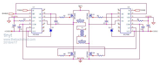 It is just a re-draw of what is in the datasheet plus my interpretation of your description. Had to interpret from English to my native language and then to drawing. So, it could be completely wrong. |
||||
| Warpspeed Guru Joined: 09/08/2007 Location: AustraliaPosts: 4406 |
That looks like it will work, but you need to ensure PWMA and PWMB have sufficient dead time. There must be a slight pause between when one goes off and the other turns on. That can either be in software, or hardware, but it must be there. Cheers, ĀTony. |
||||
| poida Guru Joined: 02/02/2017 Location: AustraliaPosts: 1480 |
tinyt: no, not like that. For this to work: U1 will drive switches Q2 and Q3 with U1 pin 6 connected to Q3 (LOW side) and U1 pin 12 connected to Q2 (HIGH side) of the bridge. U2 will drive switches Q1 and Q4 Already you have correct pin12 going to Q1 You need U2 pin 6 going to Q4 It does not matter if you have U1 taking the 50Hz signal or U2. All else in the drawing seems OK. If you have access to a dual channel oscilloscope I highly recommend that you explore the output of both the 50Hz and 20kHz PWM. Just spend $10 or so on an Arduino clone, load my code and look at the signals coming out of it. Arduino Uno pin functions running the above code: pin 5 is ENABLE pin 7 is 50Hz gate drive signal pin 9 is 20Khz PWM gate drive signal pin 6 is a utility output used for measuring code execution timing and is not used by the inverter pin 8 is pulled up to 5V internally by the micro and is the inverter run/stop control Use a momentary contact normally open switch. I use the code sbi(PORTD,6); instead of digitalWrite(6,HIGH); since it is about 100x faster cbi(PORTD,6); is the same as digitalWrite(6,LOW); Subtract pin 7 output from pin 9 from the other using the scope's math function and it will become clear how this works. Place a simple passive RC low pass filter in the signal path from Arduino to scope input. 100uF and 2K resistor might give a good smooth result. Have a look at a post I made here attempting to illustrate how PWM generated sine waves are produced here wronger than a phone book full of wrong phone numbers |
||||
| poida Guru Joined: 02/02/2017 Location: AustraliaPosts: 1480 |
Tinyt, dead time will be taken care of automatically due to the design of the IR21844 chip. With zero resistance of dead time setting pin 4 that is connected to ground (pin 3) the dead time will be about 400nS 200K ohms will give about 5uS. I set it at about 1uS in my current design. As a first approximation, just ground pin 4 to set DT to 400nS and see what happens. Again, the value of having a modern DSO is clear because you can hook up both LO and HO outputs to the scope and see the complimentary outputs and dead time. wronger than a phone book full of wrong phone numbers |
||||
| Warpspeed Guru Joined: 09/08/2007 Location: AustraliaPosts: 4406 |
I confused the IR21844 with the IR2184. The 44 has built in adjustable dead time, the 4 does not. Cheers, ĀTony. |
||||
| noneyabussiness Guru Joined: 31/07/2017 Location: AustraliaPosts: 527 |
And obviously there is no issue with the complementary being on longer than the high side.. or am I missing something ( sorry im a little slow on the best of days) I think it works !! |
||||
| Page 1 of 7 |
|||||
| The Back Shed's forum code is written, and hosted, in Australia. | © JAQ Software 2026 |
