
|
|
Forum Index : Microcontroller and PC projects : PIO explained PICOMITE
| Author | Message | ||||
| Volhout Guru Joined: 05/03/2018 Location: NetherlandsPosts: 5923 |
This is extra information, not related to the above exercises. Just for your information. There are also shift registers that need a clock pulse during the load. Such a device is the HEF4014 (and 74LS166). I have done the above analysis for the HEF4014. Not that it is of much value, the chip is near obsolete... 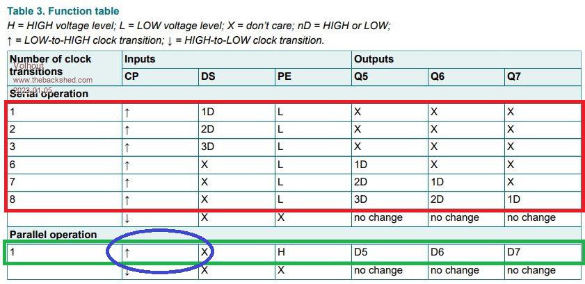 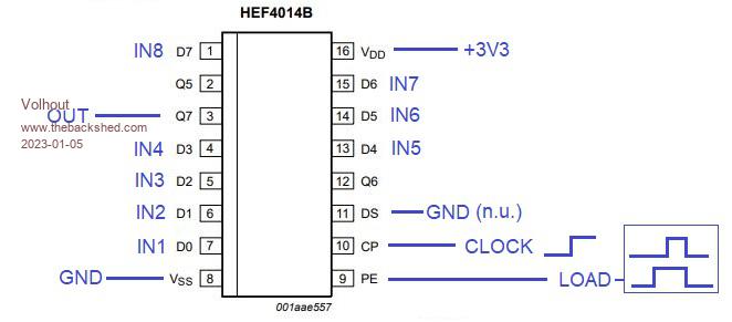 Generating a clock pulse inside the load puls is just 1 or 2 extra instructions for the PIO. This is easy. Happy programming... Edited 2023-01-05 06:42 by Volhout PicomiteVGA PETSCII ROBOTS |
||||
| JohnS Guru Joined: 18/11/2011 Location: United KingdomPosts: 4334 |
I'm being stupid I expect but doesn't that input only 7 bits? John Edited 2023-01-05 08:12 by JohnS |
||||
| phil99 Guru Joined: 11/02/2018 Location: AustraliaPosts: 3288 |
Presumably "' when counter > 0 jump to label2" should be read as ' after counter = 0 jump to label2 or ' when counter < 0 jump to label2 |
||||
| Volhout Guru Joined: 05/03/2018 Location: NetherlandsPosts: 5923 |
Hi Phil99, Note that you need only 7 clock pulses for this application. After the load pulse, you immediately have access to data on Q7 pin (OUT) representing the D7 input pin (IN 8). The first pulse will give D6 on that pin. etc. The 7'th pulse will give the D0 at pin Q7. Hence the X register is loaded with value 7. And when it decrements to 0, the 7 pulses have passed. Volhout Edited 2023-01-05 18:04 by Volhout PicomiteVGA PETSCII ROBOTS |
||||
| JohnS Guru Joined: 18/11/2011 Location: United KingdomPosts: 4334 |
But don't you need 8 of the ' shift 1 bit in instructions to be done? John |
||||
| matherp Guru Joined: 11/12/2012 Location: United KingdomPosts: 11488 |
No because the x register is post decremented after the jmp is registered x=7 shift in 1 if x<>0 jmp x=x-1 x=6 shift in 2 if x<>0 jmp x=x-1 x=5 shift in 3 if x<>0 jmp x=x-1 x=4 shift in 4 if x<>0 jmp x=x-1 x=3 shift in 5 if x<>0 jmp x=x-1 x=2 shift in 6 if x<>0 jmp x=x-1 x=1 shift in 7 if x<>0 jmp x=x-1 x=0 shift in 8 if x<>0 jmp done |
||||
| JohnS Guru Joined: 18/11/2011 Location: United KingdomPosts: 4334 |
THAT was all I needed to know, thanks. Hugely less than obvious (to me). John |
||||
| Volhout Guru Joined: 05/03/2018 Location: NetherlandsPosts: 5923 |
If you have tried to solve exercise 2 (using side set) and have found obstacles, attached is a ZIP file containing a possible solution. There are 2 things to note: 1/ In case you use SIDE SET for 2 GPx pins, you loose 2 bits in the DELAY parameter. So the maximum delay (in the last JMP) will be 7 (&b111). 2/ As of MMBasic version 5.07.06RC1 the EXECCTRL helper has been repaired. Peter has standardized that pin designations must be written as GPx. And number of pins as an integer number. The only exception was the EXECCTRL helper. Previously the conditional JMP pin needed an integer value. This is now aligned. prior to V50706RC1: EXECCTRL 0,0,&h1f now with V50706RC1: EXECCTRL GP0,0,&h1f Both options are in the listing, but I suggest you update to the new standard (the RC1 version), since I will. @Mick (Mixtel90): can you scan through the exercises and make the adaptations. When the document will be released, there will be a officiel V50706 on Geoff's website, and people will need the correct MMBasic program to try. The EXECCTRL is introduced in chapter 4 with the WRAP/WRAP TARGET. 4021_fast.zip Volhout P.S. The attached code generates 8 clocks, the last one is not actually used, since it is overruled by a load pulse before reading the data. Edited 2023-01-05 23:34 by Volhout PicomiteVGA PETSCII ROBOTS |
||||
| Pluto Guru Joined: 09/06/2017 Location: FinlandPosts: 411 |
Modified Volhout's code for HEF4021. Now it works with MM74HC165. option list PicoMite MMBasic Version 5.07.06b9 OPTION FLASH SIZE 4194304 OPTION CPUSPEED (KHz) 126000 > RUN 11100001 11100001 11100001 11100001 11100001 > H=G=F=1 E=D=C=B=0 A=1 Please note that the code is not run on the latest firmware yet. 'Volhout's PIO training: 9 'Chapter 9: shift register ISR and serial data in. 'HEF4021 och MM74HC165 Shift Register 'Volhout's PIO for HEF4021 modified for MM74HC165. ' -Changed polarity of LOAD. See modifications in PIO program lines. ' HC165 PicoMite ' pin1 GP1 ' pin2 GP0 ' pin9 GP2 ' pin10 GND ' pin15 GND ' pin16 +3.3V ' pin8 GND ' pins 3...6 & 11...14 connected either to gnd or +3.3V for testing. 'disconnect ARM from GP0/1/2 setpin gp0,pio1 'clock setpin gp1,pio1 'load setpin gp2,pio1 'data in 'configure pio1 p=Pio(pinctrl 0,2,,gp2,,gp0,) 'GP0,GP1 out, GP2 IN f=1e5 '100kHz s=PIO(shiftctrl 0,0,0,0,0,0) 'shift in from LSB for IN (and OUT) 'address code mnemonics comment ' 0 E083 SET pindirs 00011 set GP0, GP1 output ' 1 E000 SET GP1=0 GP0=0 initialize clock and load low ' 2 4060 IN NULL, 32 set ISR to 0 by shifting 32 NULL bits into it ' 3 E027 SET X=7 set counter to 7 ' 4 E002 SET GP1=1 GP0=0 start load pulse ' 5 E000 SET GP1=0 GP0=0 end load pulse ' 6 4001 IN 1 bit shift in 1 bit from GP2 ' 7 E001 SET GP1=0 GP0=1 start clock pulse ' 8 E000 SET GP1=0 GP0=0 end clock pulse ' 9 0046 JMP X-- 6 decrement X and jump to 3 when X<>0 ' A 8000 PUSH push the ISR value into FIFO (we have all 8bits now) ' B 1F02 JMP 2, dly=31 restart the whole read cycle after 31 cycles delay (delay is just for fun....) 'program pio1 pio program line 1,0,&hE083 'pio program line 1,1,&hE000 'CD4021 pio program line 1,1,&hE003 'MM74HC165 GP1=1, GP0=1 pio program line 1,2,&h4060 pio program line 1,3,&hE027 'pio program line 1,4,&hE002 'CD4021 pio program line 1,4,&hE000 'MM74HC165 GP1=0, GP0=0 'pio program line 1,5,&hE000 'CD4021 pio program line 1,5,&hE002 'MM74HC165 GP1=1, GP0=0 pio program line 1,6,&h4001 'pio program line 1,7,&hE001 'CD4021 pio program line 1,7,&hE003 'MM74HC165 GP1=1, GP0=1 'pio program line 1,8,&hE000 'CD4021 pio program line 1,8,&hE002 'MM74HC165 GP1=1, GP0=0 pio program line 1,9,&h0046 pio program line 1,10,&h8000 pio program line 1,11,&h1F02 'write the configuration PIO init machine 1,0,f,p,,s,0 'start the pio1 code PIO start 1,0 'Check the the read data in MMBasic dim d% do pio read 1,0,1,d% print bin$(d%) pause 2000 loop END I have tested with different low/high inputs on the A...H inputs on MM74HC165 with successful results. |
||||
| Volhout Guru Joined: 05/03/2018 Location: NetherlandsPosts: 5923 |
Good job !!! The only thing that could be discussed is the E003 in line 1. Technically E002 would be best, but since it is only executed once, the spurious clock pulse generated by the E003 is negated by the load pulse 3 cycles later. Good work Pluto !! Volhout PicomiteVGA PETSCII ROBOTS |
||||
| Pluto Guru Joined: 09/06/2017 Location: FinlandPosts: 411 |
Yes, I thought about it. E002 is probably the correct solution. Since E003 worked, I didn't change it. Without your remarks about the differences between HEF4021 and HC165 load polarity, I would still struggle. Pluto |
||||
| Volhout Guru Joined: 05/03/2018 Location: NetherlandsPosts: 5923 |
Hi Pluto, I hope that after seeing the procedure I use to look at datasheets, and create functional blocks, you can apply the same to other datasheets. the basic principle is the same. Somethimes it is hard to get to the correct information, sometimes it is presented different (chineese datasheets can be confusing, especially since my chineese is virually non-existent). That is why I use in this training course only datasheets from 1 manufacturer (NXP in this case, could have used TI also). So you recognise the way the data is presented in a datasheet. The next chapter on OUT and OSR will use the same procedure. Happy computing... Volhout P.S. you told me you own HEF4014's. As an exercise you could adapt the 4021 program to 4014. That requires only 1 instruction to be added, between line 4 and 5. Make sure you correct the JMP since the code get's bigger. Every time you practise, you grow... Edited 2023-01-06 17:51 by Volhout PicomiteVGA PETSCII ROBOTS |
||||
| Pluto Guru Joined: 09/06/2017 Location: FinlandPosts: 411 |
Tried to get data from CD4014BCN (16pin PDIP old). Help needed. This Shift register does not need a separate "Load" signal. According to my understanding: a. data is read at the rising edge of the clock pulse. b. clock pulse needs to be long enough. Min 70ns. I added a delay for that. c. serial input to 4014 is not used here. Serial input connected to GND. d. paralell enable pin connected to +3.3V. Does it mean that paralell input is enabled? or is it the oppsite? 'Volhout's PIO training: 9b 'Chapter 9: shift register ISR and serial data in. 'CD4014 Shift Register 'Volhout's PIO for HEF4021 modified for CD4014. 'CD4014: ' -loading data from paralell inputs to Q8 BUF OUT (pin3) on rising edge of CLK. CD4014_Pin3=Data in to PIO1. ' -needs no load pulse (as HEF4021) ' CD4014 PicoMite ' pin10 (CLK input) GP0 clock ' pin3 (Q7 output) GP2 data in to PicoMite ' pin9 (Paralell enable) +3.3V ' pin11 (serial data in) GND ' pin16 (VDD) +3.3V ' pin8 (VSS) GND ' pins 1 & 4...7 & 13...15 connected either to GND or +3.3V for testing. Parallel data inputs. 'disconnect ARM from GP0/1/2 setpin gp0,pio1 'clock 'setpin gp1,pio1 'load setpin gp2,pio1 'data in 'configure pio1 'p=Pio(pinctrl 0,2,,gp2,,gp0,) '***HEF4021*** GP0,GP1 out, GP2 IN p=Pio(pinctrl 0,1,,gp2,,gp0,) '***CD4014*** GP0 out GP2 IN f=1e5 '100kHz s=PIO(shiftctrl 0,0,0,0,0,0) 'shift in from LSB for IN (and OUT) 'address code mnemonics comment ' 0 E081 SET pindirs 00001 set GP0 output ' 1 E000 SET GP0=0 initialize clock low ' 2 4060 IN NULL, 32 set ISR to 0 by shifting 32 NULL bits into it ' 3 E027 SET X=7 set counter to 7 ' 4 E001 SET GP0=1 start clock pulse ' 5 FF01 SET GP0=1 dly=31 (make sure that the clock pulse is long enough) ' 6 E000 SET GP0=0 end clock pulse ' 7 4001 IN 1 bit shift in 1 bit from GP2 ' 8 0044 JMP X-- 4 decrement X and jump to 4 when X<>0 ' 9 8000 PUSH push the ISR value into FIFO (we have all 8bits now) ' 10 1F02 JMP 2, dly=31 restart the whole read cycle after 31 cycles delay (delay is just for fun....) 'program pio1 pio program line 1,0,&hE081 pio program line 1,1,&hE000 pio program line 1,2,&h4060 pio program line 1,3,&hE027 pio program line 1,4,&hE001 pio program line 1,5,&hFF01 pio program line 1,6,&hE000 pio program line 1,7,&h4001 pio program line 1,8,&h0044 pio program line 1,9,&h8000 pio program line 1,10,&h1F02 'write the configuration PIO init machine 1,0,f,p,,s,0 'start the pio1 code PIO start 1,0 'Check the the read data in MMBasic dim d% do pio read 1,0,1,d% print bin$(d%) pause 200 loop END The output I get is always &b11111111 regardless of how the CD4014 inputs are set. Pluto |
||||
| Volhout Guru Joined: 05/03/2018 Location: NetherlandsPosts: 5923 |
Hi Pluto, If I look at the 4014 datasheet truth table, I see that the LOAD requires a H level on the PE pin. The SHIFT requires a L level on the PE pin. See first post of page 5 of this thread... Attached is the modified 4021 program, that works for my chip (HEF4014) tested. With the wiring as suggested in the 4014 post. 'disconnect ARM from GP0/1/2 �setpin gp0,pio1 � � � � 'clock �setpin gp1,pio1 � � � � 'load �setpin gp2,pio1 � � � � 'data in � 'configure pio1 �p=Pio(pinctrl 0,2,,gp2,,gp0,) � � � � 'GP0,GP1 out, GP2 IN �f=1e5 � � � � � � � � � � � � � � � � '100kHz �s=PIO(shiftctrl 0,0,0,0,0,0) � � � � �'shift in from LSB for IN (and OUT) � 'address � code � �mnemonics � � � � �comment ' �0 � � � E083 � �SET pindirs 00011 �set GP0, GP1 output ' �1 � � � E000 � �SET GP1=0 GP0=0 � �initialize clock and load low ' �2 � � � 4060 � �IN NULL, 32 � � � �set ISR to 0 by shifting 32 NULL bits into it ' �3 � � � E027 � �SET X=7 � � � � � �set counter to 7 ' �4 � � � E002 � �SET GP1=1 GP0=0 � �start load pulse ' �5 � � � E003 � �SET GP1=1 GP0=1 � �clock inside load puls ' �6 � � � E000 � �SET GP1=0 GP0=0 � �end load pulse ' �7 � � � 4001 � �IN 1 bit � � � � � shift in 1 bit from GP2 ' �8 � � � E001 � �SET GP1=0 GP0=1 � �start clock pulse ' �9 � � � E000 � �SET GP1=0 GP0=0 � �end clock pulse ' �A � � � 0047 � �JMP X-- 7 � � � � �decrement X and jump to 3 when X<>0 ' �B � � � 8000 � �PUSH � � � � � � � push the ISR value into FIFO (we have all 8bits now) ' �C � � � 1F02 � �JMP 2, dly=31 � � �restart the whole read cycle after 31 cycles delay (delay is just for fun....) � 'program pio1 �pio program line 1,0,&hE083 �pio program line 1,1,&hE000 �pio program line 1,2,&h4060 �pio program line 1,3,&hE027 �pio program line 1,4,&hE002 �pio program line 1,5,&hE003 � �pio program line 1,6,&hE000 �pio program line 1,7,&h4001 �pio program line 1,8,&hE001 �pio program line 1,9,&hE000 �pio program line 1,10,&h0047 �pio program line 1,11,&h8000 �pio program line 1,12,&h1F02 � � 'write the configuration �PIO init machine 1,0,f,p,,s,0 � � 'start the pio1 code �PIO start 1,0 � 'Check the the read data in MMBasic �dim d% � �do � �pio read 1,0,1,d% � �print bin$(d%) � �pause 200 �loop � END This is the waveform at CLOCK (red trace) and LOAD (blue trace) 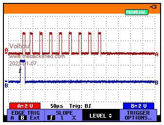 Maybe your chip is defective, but I can't understand why you came to the conclusion that you do not need a level change on the PE pin. Don't give up, I also went to bed several times in despair, and the next morning, I knew what went wrong. It is not always easy.... Volhout P.S. We run at 100kHz, that is 10us per instructions. For 70ns you do not add delay. You are 140 times slower without delay. But you added the delay correctly to the instruction.!! Edited 2023-01-07 01:15 by Volhout PicomiteVGA PETSCII ROBOTS |
||||
| Pluto Guru Joined: 09/06/2017 Location: FinlandPosts: 411 |
I thought that PE was only selection between Paralell in and serial in. That is why I connected it to 3.3V. Obviously that was a wrong interpretation of the datasheet. Sorry, I have no time to test now. Guests at the front door.  |
||||
| Pluto Guru Joined: 09/06/2017 Location: FinlandPosts: 411 |
Thanks Volhout. Your program works also on my CD4014 chip(s). They are desoldered from some old piece of equipment. Based on chip logo made by National Semiconductor. |
||||
| Pluto Guru Joined: 09/06/2017 Location: FinlandPosts: 411 |
Started to play with 74HC595 (8-bit serial-in, serial or parallel-out shift register with output latches; 3-state). In order to understand how the chip operates, I started by controlling it directly from PicoMite using PIO. Based on the datasheet (Nexperia) and some trial and error I got it working with 8 LEDs as output indicators. '74HC595 Shift Register. Serial data in, paralell data out. FN 8.1.2023. 'Testprogram before implementation of PIO-program. Just to see how the chip operates and to see which control signals 'are necessary. '***74HC595*** 'Symbol Pin Description 'Q0, Q1, Q2, Q3, Q4, Q5, Q6, Q7 15, 1, 2, 3, 4, 5, 6, 7 parallel data output 'GND 8 ground (0 V) 'Q7S 9 serial data output 'MR 10 master reset (active LOW) 'SHCP 11 shift register clock input 'STCP 12 storage register clock input 'OE 13 output enable input (active LOW) 'DS 14 serial data input 'Q0 15 parallel data output 0 'VCC 16 supply voltage ' 'Connect MR to 3.3V. 'Connect OE to GND. setpin GP0,DOUT 'shift register clock output. Connect to pin11 on 74HC595. setpin GP1,DOUT 'storage register clock output. Connect to pin12 on 74HC595. SETPIN GP2,DOUT 'serial data output. Connect to pin14 on 74HC595. 'setpin GP3,DOUT 'output enable. Connect to pin13 on 74HC595. Not needed; Connect pin13 to GND. DIM INTEGER DS 'Data to be output to DS (74HC595's serial data input) PIN(GP0)=0:PIN(GP1)=0 do FOR J=0 to 255 DS=j For i=0 to 7 'first load all data to the shift register PIN(GP2)=(DS and 2^i)>>i PIN(GP0)=1:Pin(GP0)=0 'clock pulse to shift register. Data not yet to outputs. next i 'The clock pulse to storage register could also be supplied in the previous FOR-NEXT, 'but the output LEDs are then flickering slightly during loading. Flickering occurs also when 'using Output Enable (OE) to disable output when loading starts and enable again when done. 'No flickering when first all data is loaded to the shift register and then afterwards are 'shifted into the storage register. 'Separate loading of the storage register is of course slower than simultaneous loading of both shift 'and storage register, but the led row is "cleaner". for K=0 to 7 'move the data from shift register to storage register. PIN(GP1)=1:Pin(GP1)=0 'clock pulse to storage register. Data to outputs. next K Pause 50 Next J loop END Next step was to implement the operation via PIO. The problem seems to be that I am not able to get the data from MMbasic into the PIO. The program just makes one clock pulse on GP0 followed by one clock pulse on GP1 and nothing comes out on GP2 to 74HC595. '74HC595 Shift Register. Serial data in, paralell data out. FN 8.1.2023. ' '***74HC595*** 'Symbol Pin Description 'Q0, Q1, Q2, Q3, Q4, Q5, Q6, Q7 15, 1, 2, 3, 4, 5, 6, 7 parallel data output 'GND 8 ground (0 V) 'Q7S 9 serial data output 'MR 10 master reset (active LOW) 'SHCP 11 shift register clock input 'STCP 12 storage register clock input 'OE 13 output enable input (active LOW) 'DS 14 serial data input 'Q0 15 parallel data output 0 'VCC 16 supply voltage ' 'Connect MR to 3.3V. 'Connect OE to GND. ' ' 'disconnect ARM from GP0/1/2 setpin gp0,pio1 'SHCP: shift register clock output. Connect to pin11 on 74HC595. setpin gp1,pio1 'STCP: storage register clock output. Connect to pin12 on 74HC595. setpin gp2,pio1 'DS: serial data output. Connect to pin14 on 74HC595. 'configure pio1 p=Pio(pinctrl 0,2,1,,,GP0,GP2) 'GP0,GP1 SET pins, 1 out pin GP2 f=1e5 '100kHz s=PIO(shiftctrl 0,0,0,0,0,0) 'shift in from LSB for IN (and OUT) 'address code mnemonics comment ' 0 111 00000 100 00011 SET pindirs 00011 set GP0, GP1 output ' 1 111 00000 000 00000 SET GP1=0 GP0=0 initialize clock and load low ' 2 111 00000 001 00111 SET X=7 set counter to 7 ' 3 100 00000 101 00000 PULL:load 32bit word from TX-FIFO into OSR. Stall if FIFO is empty. ' 4 011 00000 000 00001 OUT: Shift bits out from OSR to dest: GP2 ' 5 111 00000 000 00001 SET GP0=1 shift register clock. Start pulse. ' 6 111 00000 000 00000 SET GP0=0 shift register clock. Stop pulse. ' 7 111 00000 000 00010 SET GP1=1 storage register clock. Start pulse. ' 8 111 00000 000 00000 SET GP1=0 storage register clock. Stop pulse. ' 9 000 00000 010 00011 JMP X-- 3 decrement X and jump to 2 when X<>0 ' 10 000 11111 000 00010 JMP 2, dly=31. Restart the whole cycle after 31 cycles delay (delay is just for fun....) 'program pio1 ' &b***-----***----- pio program line 1, 0,&b1110000010000011 pio program line 1, 1,&b1110000000000000 pio program line 1, 2,&b1110000000100111 pio program line 1, 3,&b1000000010100000 pio program line 1, 4,&b0110000000000001 pio program line 1, 5,&b1110000000000001 ' &b***-----***----- pio program line 1, 6,&b1110000000000000 pio program line 1, 7,&b1110000000000010 pio program line 1, 8,&b1110000000000000 pio program line 1, 9,&b0000000001000011 pio program line 1,10,&b0001111100000010 'write the configuration PIO init machine 1,0,f,p,,s,0 'start the pio1 code PIO start 1,0 'Check the the read data in MMBasic dim integer d% do d%=0 do d%=d%+1 pio WRITE 1,0,1,d% print bin$(d%,8) pause 100 Loop while d%<256 loop END Obviously I am doing something stupid when trying to move MMbasic-> TX_FIFO -> OSR -> PIO. Gretful for any hints...or maybe I should wait for next lesson from Volhout's PIO-Academy? |
||||
| Pluto Guru Joined: 09/06/2017 Location: FinlandPosts: 411 |
Re: The tests in previous mail. option list PicoMite MMBasic Version 5.07.06 OPTION FLASH SIZE 4194304 > |
||||
| Volhout Guru Joined: 05/03/2018 Location: NetherlandsPosts: 5923 |
Hi Pluto, I will look into this but due to hospital visit I will respond tuesday night soonest. I am very happy you tried. This is the right spirit. Most unfortunate I cannot debug your code sooner. I can imagine you are just jumping to get on with the PIO.. It looks like your code does generate 1 clock per 1 latch pulse. Between the clock and the latch pulse should be the conditional jump (decrement X) instructions. So line 9 should move between 6 and 7. Volhout Edited 2023-01-09 19:13 by Volhout PicomiteVGA PETSCII ROBOTS |
||||
| Pluto Guru Joined: 09/06/2017 Location: FinlandPosts: 411 |
Volhout, take care. I am not in a hurry. I will keep on trying, but in between I have to shuffle snow. Pluto |
||||
| The Back Shed's forum code is written, and hosted, in Australia. | © JAQ Software 2026 |
