
|
|
Forum Index : Microcontroller and PC projects : PIO explained PICOMITE
| Author | Message | ||||
| phil99 Guru Joined: 11/02/2018 Location: AustraliaPosts: 1793 |
Other ways to play with 74HC595 chips. HC595 |
||||
| Pluto Guru Joined: 09/06/2017 Location: FinlandPosts: 330 |
Fially I got the 74HC595 PIO program to work. Maybe not the most elegant solution. '74HC595 Shift Register. Serial data in, paralell data out. FN 9.1.2023. ' '***74HC595*** 'Symbol Pin Description 'Q0, Q1, Q2, Q3, Q4, Q5, Q6, Q7 15, 1, 2, 3, 4, 5, 6, 7 parallel data output 'GND 8 ground (0 V) 'Q7S 9 serial data output 'MR 10 master reset (active LOW) 'SHCP 11 shift register clock input 'STCP 12 storage register clock input 'OE 13 output enable input (active LOW) 'DS 14 serial data input 'Q0 15 parallel data output 0 'VCC 16 supply voltage ' 'Connect MR to 3.3V. 'Connect OE to GND. ' ' 'disconnect ARM from GP0/1/2 setpin gp0,pio1 'SHCP: shift register clock output. Connect to pin11 on 74HC595. setpin gp1,pio1 'STCP: storage register clock output. Connect to pin12 on 74HC595. setpin gp2,pio1 'DS: serial data output. Connect to pin14 on 74HC595. 'configure pio1 p=Pio(pinctrl 1,3,1,,GP0,GP0,GP2) '1 sideset pin:GP0. 3 SET pins: GP0,GP1,GP2. 1 OUT pin GP2 f=1e5 '100kHz s=PIO(shiftctrl 0,0,0,0,0,1) 'shift in from LSB for IN (and OUT) 'SHIFTCTRL: shift out of OSR to the right; LSB first. 'program pio1 ' &b***-----***----- pio program line 1, 0,&b1110000010000111 'SET pindirs GP2,GP1 and GP0 pio program line 1, 1,&b1110000000000000 'SET GP1=0 sideset:GP0=0. Initialize both clocks low. pio program line 1, 2,&b1110000000100111 'SET X=7 pio program line 1, 3,&b1000000010100000 'PULL:load 32bit word from TX-FIFO into OSR. Stall if FIFO is empty. pio program line 1, 4,&b0111000000000001 'OUT: Shift bits out from OSR to dest: GP2. Side-set GP0=1 start shift clk pulse. ' &b***-----***----- pio program line 1, 5,&b1110000000000010 'SET GP1=1 storage reg clk Start pulse. Side-set GP0=0 stop shift clk pulse. pio program line 1, 6,&b1110000000000000 'SET GP1=0 storage register clock. Stop pulse. pio program line 1, 7,&b0000000001000100 'JMP X-- 4. decrement X and jump to 2 when X<>0. pio program line 1, 8,&b0000111100000010 'JMP 2. JMP 2, dly=31. Restart the whole cycle after 15 cycles delay. ' &b***-----***----- 'write the configuration PIO init machine 1,0,f,p,,s,0 'start the pio1 code PIO start 1,0 'Check the the read data in MMBasic dim integer d% do d%=0 do d%=d%+1 pio WRITE 1,0,1,d% print bin$(d%,8) pause 200 Loop while d%<256 loop END |
||||
| Volhout Guru Joined: 05/03/2018 Location: NetherlandsPosts: 3555 |
Hi Pluto, I am not sure why it works. I notice that at every clock pulse you also issue a latch pulse. There is technically no objection, but normal you would only change the output when a full set of 8 bits is received. In your code every LED lights at every bit while shifting in. I have been able to make your code work on my breadboard when I make following change: 'program pio1 ' � � � � � � � � � � �&b***-----***----- �pio program line 1, 0,&b1110000010000111 'SET pindirs GP2,GP1 and GP0 �pio program line 1, 1,&b1110000000000000 'SET GP1=0 sideset:GP0=0. Initialize both clocks low. �pio program line 1, 2,&b1110000000100111 'SET X=7 �pio program line 1, 3,&b1000000010100000 'PULL:load 32bit word from TX-FIFO into OSR. Stall if FIFO is empty. �pio program line 1, 4,&b0111000000000001 'OUT: Shift bits out from OSR to dest: GP2. Side-set GP0=1 start shift clk pulse. �pio program line 1, 5,&b0000000001000100 'JMP X-- 4. decrement X and jump to 4 when X<>0. �pio program line 1, 6,&b1110000000000010 'SET GP1=1 storage reg clk Start pulse. Side-set GP0=0 stop shift clk pulse. �pio program line 1, 7,&b1110000000000000 'SET GP1=0 storage register clock. Stop pulse. �pio program line 1, 8,&b0000111100000010 'JMP 2. JMP 2, dly=31. Restart the whole cycle after 15 cycles delay. ' � � � � � � � � � � �&b***-----***----- But honestly I do not like the code in line 4. In one instruction you shift out data AND you have the rising clock pulse. I know it is in the RP2040 datasheet that the SIDE SET happens later than the other parts of the instruction, but given that the pico PIO is so fast (can run at 250MHz) and the 595 shift register is limited to some 40MHz, there is a good chance that the timing is critical for the 595. The data needs to be stable (called "set up time" before the rising edge of the shift clock). So.. it works.. but I suggest to do the rising clock edge in an instruction after the OSR shift instruction. To guarantee a controlled (by PIO clock) setup time. Volhout Edited 2023-01-10 05:35 by Volhout PicomiteVGA PETSCII ROBOTS |
||||
| Pluto Guru Joined: 09/06/2017 Location: FinlandPosts: 330 |
Changed operation: 1. clocking in the bits into the Shift Register from OSR. 2. clocking in the bits to Storage Register from Shift Register. This gives smoother transition on the LEDs. No flickering of the LEDs when output is changed. Remains still a problem. LSB of the data is present on 74HC595 Q7 and MSB sets Q0. Have struggled to get reverse order (LSB=Q0..MSB=Q7), but without success. I think this order would be more logical. '74HC595 Shift Register. Serial data in, paralell data out. FN 9.1.2023. ' '***74HC595*** 'Symbol Pin Description 'Q0, Q1, Q2, Q3, Q4, Q5, Q6, Q7 15, 1, 2, 3, 4, 5, 6, 7 parallel data output 'GND 8 ground (0 V) 'Q7S 9 serial data output 'MR 10 master reset (active LOW) 'SHCP 11 shift register clock input 'STCP 12 storage register clock input 'OE 13 output enable input (active LOW) 'DS 14 serial data input 'Q0 15 parallel data output 0 'VCC 16 supply voltage ' 'Connect MR to 3.3V. 'Connect OE to GND. ' ' 'disconnect ARM from GP0/1/2 setpin gp0,pio1 'SHCP: shift register clock output. Connect to pin11 on 74HC595. setpin gp1,pio1 'STCP: storage register clock output. Connect to pin12 on 74HC595. setpin gp2,pio1 'DS: serial data output. Connect to pin14 on 74HC595. 'configure pio1 p=Pio(pinctrl 1,3,1,,GP0,GP0,GP2) '1 sideset pin:GP0. 3 SET pins: GP0,GP1,GP2. 1 OUT pin GP2 f=1e5 '100kHz s=PIO(shiftctrl 0,8,0,1,0,1) 'shift in from LSB for IN (and OUT) 'SHIFTCTRL: shift out of OSR to the right; LSB first. Please note that LSB will set 74HC595 Q7 and MSB sets Q0. 'Have struggled to get reverse order (LSB=Q0..MSB=Q7), but without success. I think that this order would be 'more logical. 'program pio1 ' &b***-----***----- pio program line 1, 0,&b1110000010000111 'SET pindirs GP2,GP1 and GP0. Also OUT pin GP2. pio program line 1, 1,&b1110000000000000 'SET GP1=0 sideset:GP0=0. Initialize both clocks low. ' &b***-----***----- pio program line 1, 2,&b1110000000100111 'SET X=7. Counter for Shift reg clk pulses. Count down 7...0. pio program line 1, 3,&b1000000011100000 'PULL:load 32bit word from TX-FIFO into OSR. Stall if FIFO is empty. ' &b***-----***----- pio program line 1, 4,&b0111000000000001 'OUT: Shift bits out from OSR to dest: GP2. Side-set GP0=1 start shift clk pulse. pio program line 1, 5,&b0000000001000100 'JMP X-- 4. decrement X and jump to 4 when X<>0. 'Storage register clocking after all bits are shifted into Shift register. This gives LED transitions w/o flickering. 'Side-set GP0=0 for all subsequent instructions; Shift reg clk inactive. pio program line 1, 6,&b1110000001000111 'SET Y=7. Counter for Storage reg clk pulses. Count down 7...0. ' &b***-----***----- pio program line 1, 7,&b1110000000000010 'SET GP1=1 storage reg clk Start pulse. Side-set GP0=0 stop shift clk pulse. pio program line 1, 8,&b1110000000000000 'SET GP1=0 storage register clock. Stop pulse. ' &b***-----***----- pio program line 1, 9,&b0000000010000111 'JMP Y-- 7. decrement Y and jump to 7 when Y<>0. pio program line 1,10,&b0000111100000010 'JMP 2. JMP 2, dly=15. Restart the whole cycle after 15 cycles delay. ' &b***-----***----- 'write the configuration PIO init machine 1,0,f,p,,s,0 'start the pio1 code PIO start 1,0 'Check the the read data in MMBasic dim integer d% do d%=0 do d%=d%+1 'Out32bit=d%+d%<<8+d%<<16+d%<<24 pio WRITE 1,0,1,d% print bin$(d%,8) pause 200 Loop while d%<256 loop END |
||||
| Pluto Guru Joined: 09/06/2017 Location: FinlandPosts: 330 |
Sorry Volhout, I did not see your post before I posted my latest program version! |
||||
| Volhout Guru Joined: 05/03/2018 Location: NetherlandsPosts: 3555 |
Chapter 10: Shift out data from OSR to a 74HC595 shift register Serial peripherals can extend the functionality of a microcontroller. Such devices can be DAC's (digitial to analog converters), shift registers, but also ethernet chips. The PIO can assist in communication with these devices. For most, if not all, of these serial protocols, the OSR (Output Shift Register) is used. This is the output equivalent of the ISR (Input Shift Register) we have used in several earlier experiments. Of coarse we need to write data into the OSR before it can shift data to the peripheral. The data path looks like this: MMBasic ---> Output FIFO ---> OSR ----> GPx pins. To get data into the output FIFO we use the MMBasic PIO WRITE function. PIO WRITE a,b,c,d a/ the PIO (in out examples PIO 1) b/ the state machine (0...3) c/ the number of 32 bit values to write (1..4) d/ the integer variable that supplies the data (can be an array in case multiple 32 bit words are send). Once the data is written in the FIFO the PIO can fetch the data using the PULL instruction  The PULL instruction has a few flags and a delay parameter. DELAY/SIDE SET : we have discussed this before IfEMpty: we will not discuss this here Block: When 1 the PULL instruction halts the PIO until there is data to pull from FIFO. We have used the BLOCK flag in an earlier exercise where we generated the GATE signal for the frequency counter. To shift data out to the IO pins, the OUT instruction is used. The paramaters are listed below.  DELAY/SIDE SET: already discussed earlier. DESTINATION: "000" for PINS, "001" = X, "100" = PINDIRS, "011"=NULL (shift data lost) BITCOUNT: the number of bits to shift out. So it is pretty obvious to us how we can shift out 1 bit of data to pins. Use the OUT instruction, destination "000", and number of bit = 1 But there is something specific we need to do to assign a GPx pin to the OSR. The OUT instruction has it's own configuration in PINCTRL. PINCTRL a,b,c,d,e,f,g a/ number of side set pins b/ number of set pins c/ number of OUT pins.....this is new, we have neve used this before d/ GP pin base for IN e/ GP pin base for side set f/ GP pin base for set g/ GP pin base for OUT.....this is new, we have not used this before. To explain how these puzzle pieces fit together we will explain using a concrete application: sending data to a 74HC595 shift register.. Similar to chapter 9 we will use the datasheet to determine how we can send serial data to the chip. The 74HC595 contains a set of 8 shift in registers, shifting happens on the rising edge of the SHCP (CLOCK)signal. The input data must be supplied to the DS (DATA) pin. Once all 8 bits are clocked in, the data is latched (frozen solid) into the 8 output registers at a rising edge fo the STCP (LATCH) signal. When MRn is set low, the register is cleared. In out case we do not drive that pin, we tie it high, but many applications will use this pin to ensure a controlled power up (reset at power up). OEn must be low to provide data to the output pins.  Above information results in below connection diagram for the chip.  The PIO program to send data to the 74HC595 must do following: 'set CLOCK, LATCH, DATA to output 'set CLOCK=low, LATCH=low (and DATA=low) 'label1: 'set variable X (counter) to 7 'PULL data in OSR, blocking (halt here when no new data) 'label2: 'shift 1 bit OSR -> GPx (send data to 595 SER pin) 'generate CLOCK pulse (low->high->low) 'check X<>0 and JMP to label 2 when not 0, post decrement X 'generate LATCH pulse (low -> high -> low) 'JMP to label1 It must be said that there is no explicit requirement for the LATCH and CLOCK to become low again as separate instructions. But for clarity here we do so. Also note that we store the value 7 in the counter. For this register we need to provide a clock pulse to get data in the first shift register. So for 8 bits we need 8 clocks. Let's assign GP pins: CLOCK = GP0, LATCH = GP1, DATA = GP2 GP0 and GP1 will be controlled from SET instructions, GP2 from the OUT instruction. So this gives following configuration(see above): PINCTRL 0,2,1,,,GP0,GP2 One last thing to configure is the shift direction. The OSR can shift left (OUT_SHIFTDIR=0) where the MSB is shifted out first, and can shift right (OUT_SHIFTDIR=1) where the LSB is shifted out first. This is determined using the SHIFTCTRL register. SHIFTCTRL a,b,c,d,e,f a/...d/ set to 0, not used here e/ IN_SHIFTDIR (explainer earlier) f/ OUT_SHIFTDIR (see above). Now we have a dilema. When we choose "shift right" the OSR LSB is shifted out first, but will (after 8 clock pulses) end up at Q7 (the shift registers MSB). When we choose "shift left" the OSR MSB (bit 31) is shifted out first, and will end up at Q7 of the 74HC595 after 8 clock pulses. So what now...?? There are 3 options: 1/ shift left all 32 bits from the OSR to the HC595. Bits 31...8 will be clocked "through" the register, and bits 7...0 will end up at shift regsiter outputs Q7...Q0 2/ shift right 8 bits to the shift register,, and connect the 595 outputs in reverse order. Q7=out1, Q6=out2....Q0=out8 3/ Dummy shift left 24 bits OSR to no-where, then left shift the remaining 8 OSR bits to the 74HC595. Option 2 is prototyped by Pluto (see listing in previous posts) Before we start with investigating the other 2 options, there is one thing that needs attention. In out previous examples we always started out with defining the pin direction. And we have always been doing that using the SET command, with destination PINDIRS. We can do that for all pins that are member of the SET group. But the pin that we use to send serial data out is member of the OUT group. That is a different group. Sometimes you are lucky, and you can extend the SET group to also cover the OUT pin. But there is a catch (and that is a problem in our case). When we send serial data out using the OUT command, and in the next instruction want to SET the clock pin high, we hard set all pins in the SET group. Also the OUT pin is re-written to the value int he SET command. The OUT pin can therefore not be a member of the SET group, or (as Pluto shows in his solution) we cannot use SET to set the clock high. We use SIDE SET. Pluto's solution is technically a better solution. But for educational purpose we show how it can be done when OUT is not a member of the SET group. There is another possibility to set the pin direction of a pin. Use the OUT instruction itself. If you look above in the field description, you can see that the OUT instruction can also have PINDIRS as a destination. If you shift OUT a "1" into the PINDIRS, then the pin that is base for the OUT group (GP2 in our case) is also changed into an output. OUT pindirs 1 = 011 00000 100 00001 = 0110 0000 1000 0001 = &h6081 But we can only shift a logic "1" out OSR when there is a logic "1" in OSR. So first we have to program OSR with a "1". That may not be easy, but we can (in 1 instruction) fill OSR with all 1's, by MOV'ing an inverted NULL in it.  DESTINATION: "111" = OSR OPERATION: "01" = INVERT SOURCE: "011" = NULL MOV -NULL-> OSR = 101 00000 111 01 011 = 1010 0000 1110 1011 = &hA0EB Now let's look at option 1: SHIFT 32 bits to the 8 bit shift register, but since bits 31...8 are shifted through, only bits 7..0 remain in the shift register when the latch puls happens. Together with the well known SET of the pin direction of the SET pins the complete program for shifting data to the 74HC595 looks like: 'disconnect ARM from GP0/1/2 �setpin gp0,pio1 � � � � 'clock �setpin gp1,pio1 � � � � 'load �setpin gp2,pio1 � � � � 'data in � 'configure pio1 �p=Pio(pinctrl 0,2,1,,,gp0,gp2) � � � �'GP0,GP1 SET, GP2 OUT �f=1e5 � � � � � � � � � � � � � � � � '100kHz �s=PIO(shiftctrl 0,0,0,0,0,0) � � � � �'shift OUT through MSB, (shift in from LSB) � 'address � �code � �mnemonics � � � � comment ' �0 � � �E083 � �SET pindirs 00011 � set GP0 GP1 GP2 output ' �1 � � �E000 � �SET GP1=0 GP0=0 � � initialize clock and load low ' �2 � � �A0EB � �MOV -1 -> OSR � � � OSR = &hffffffff ' �3 � � �6081 � �OUT pindirs 1 � � � SET GP2 output (shif 1 bit logic 1 into pindir) � ' �4 � � �E03F � �SET X=31 � � � � � �go through al 32 bits (31...0) ' �5 � � �80A0 � �PULL OSR blocking � wait for data in FIFO and load in OSR ' �6 � � �6001 � �OUT GP2, 1 � � � � �send 1 bit to GP2 ' �7 � � �E001 � �SET GP0=1, GP1=0 � �rising edge clock ' �8 � � �E000 � �SET GP0=0, GP1=0 � �falling edge clock ' �9 � � �0046 � �JMP X-- 6 � � � � � jump to 6 when X<>0, post decrement X � ' �A � � �E002 � �SET GP0=0 GP1=1 � � start latch pulse ' �B � � �E000 � �SET GP0=0 GP1=0 � � end latch pulse ' �C � � �0004 � �JMP 4 � � � � � � � restart the whole shift cycle � � 'program pio1 �pio program line 1,0,&hE083 �pio program line 1,1,&hE000 �pio program line 1,2,&hA0EB �pio program line 1,3,&h6081 �pio program line 1,4,&hE03F �pio program line 1,5,&h80A0 �pio program line 1,6,&h6001 �pio program line 1,7,&hE001 �pio program line 1,8,&hE000 �pio program line 1,9,&h0046 �pio program line 1,10,&hE002 �pio program line 1,11,&hE000 �pio program line 1,12,&h0004 � � 'write the configuration �PIO init machine 1,0,f,p,,s,0 � � 'start the pio1 code �PIO start 1,0 � 'Check the the read data in MMBasic �dim d% � �do � �for i%=0 to 255 � � �PIO WRITE 1,0,1,i% � � �pause 20 � �next i% �loop � END This code works well, but "wastes" 24 of the 32 clock cycles sending useless data. There is a trick to avoid that. Once we have the data in OSR we can (in one instruction) shift 24 bits into oblivion (called: NULL), and shift the remaining 8 bits to the 74HC595. DESTINATION = "011" = NULL BITS = "11000" = 24 OUT OSR->NULL 24 = 011 00000 011 11000 = 0110 0000 0111 1000 = &h6078 The modified program looks like this: 'disconnect ARM from GP0/1/2 �setpin gp0,pio1 � � � � 'clock �setpin gp1,pio1 � � � � 'load �setpin gp2,pio1 � � � � 'data in � 'configure pio1 �p=Pio(pinctrl 0,2,1,,,gp0,gp2) � � � �'GP0,GP1 SET, GP2 OUT �f=1e5 � � � � � � � � � � � � � � � � '100kHz �s=PIO(shiftctrl 0,0,0,0,0,0) � � � � �'shift OUT through MSB, (shift in from LSB) � 'address � �code � �mnemonics � � � � comment ' �0 � � �E083 � �SET pindirs 00011 � set GP0 GP1 GP2 output ' �1 � � �E000 � �SET GP1=0 GP0=0 � � initialize clock and load low ' �2 � � �A0EB � �MOV -1 -> OSR � � � OSR = &hffffffff ' �3 � � �6081 � �OUT pindirs 1 � � � SET GP2 output (shif 1 bit logic 1 into pindir) � ' �4 � � �E027 � �SET X=7 � � � � � � go through al 32 bits (31...0) ' �5 � � �80A0 � �PULL OSR blocking � wait for data in FIFO and load in OSR ' �6 � � �6078 � �OUT OSR->NULL, 24 � shift data in OSR 24 bits ' �7 � � �6001 � �OUT GP2, 1 � � � � �send 1 bit to GP2 ' �8 � � �E001 � �SET GP0=1, GP1=0 � �rising edge clock ' �9 � � �E000 � �SET GP0=0, GP1=0 � �falling edge clock ' �A � � �0047 � �JMP X-- 7 � � � � � jump to 7 when X<>0, post decrement X � ' �A � � �E002 � �SET GP0=0 GP1=1 � � start latch pulse ' �B � � �E000 � �SET GP0=0 GP1=0 � � end latch pulse ' �C � � �0004 � �JMP 4 � � � � � � � restart the whole shift cycle � � 'program pio1 �pio program line 1,0,&hE083 �pio program line 1,1,&hE000 �pio program line 1,2,&hA0EB �pio program line 1,3,&h6081 �pio program line 1,4,&hE027 �pio program line 1,5,&h80A0 �pio program line 1,6,&h6078 �pio program line 1,7,&h6001 �pio program line 1,8,&hE001 �pio program line 1,9,&hE000 �pio program line 1,10,&h0047 �pio program line 1,11,&hE002 �pio program line 1,12,&hE000 �pio program line 1,13,&h0004 � � 'write the configuration �PIO init machine 1,0,f,p,,s,0 � � 'start the pio1 code �PIO start 1,0 � 'Check the the read data in MMBasic �dim d% � �do � �for i%=0 to 255 � � �PIO WRITE 1,0,1,i% � � �pause 20 � �next i% �loop � END That was a lot of theory. For thos who want to look further: it is definitely possible to compact this code much further, or re-write it to use the SIDE SET (as Pluto did). Play with it, and enjoy.... For now this is the end of the series. I will occasionally post further posts in this thread, such as a more completed multifunction counter, and may explain some of the project that are worth diving into. I thank you all for your continued attention, ans supportive posts. That has been very helpfull. Whenever you write something, let me know... Volhout g/ Edited 2023-01-10 08:17 by Volhout PicomiteVGA PETSCII ROBOTS |
||||
| Pluto Guru Joined: 09/06/2017 Location: FinlandPosts: 330 |
Volhout, Re operation at high frequency. Your program is OK at least up to 100MHz PIO frequency. Tested also my version, which is OK up to 40MHz. At higher f errors are visible on the LEDS. Re load pulse (Storage Register Clk, STCP). I misunderstood the datasheet. Thought that a separate pulse was needed for each bit. I was in fact reloading the 8 databits 8 times. After the Shift Register is loaded, one load pulse (STCP) is enough to transfer all bits to to the storage register and the outputs. Re the order of data on the outputs. You solution with sending the unnecessary 24 bits to the NULL-register correctly outputs LSB on output Q0....MSB on Q7.  Your PIO training lessons have really demystified the usage of PIO! Before your lessons I tried to understand the use of PIO by reading the RP2040 manual; It only made me more confused. Now I can find some useful info from the manual, but the concrete examples in "PIO explained PICOMITE by Volhout" is my PIO Bible. Thanks /Pluto |
||||
| JohnS Guru Joined: 18/11/2011 Location: United KingdomPosts: 3661 |
595 SER pin being DS - right? John |
||||
| Volhout Guru Joined: 05/03/2018 Location: NetherlandsPosts: 3555 |
Thanks Pluto ! I am actually blushing now... Reason for the series was actually the demystifiction of the PIO blocks. The basis under it is actually simple (although you can make it very complex in just a few instructions). But the RP2040 manual (despite being a holy bible on the PIO core itself) confuses as soon as you start using it for a different environment as their beloved python. Although we have not touched all aspects, there is a basis that MMBasic users can work with. Let's be honest, most of the examples and exercises could also be written in MMBasic, or use the peripherals available to MMBasic. But PIO can also do things that are not available in standard peripherals (such as generating VGA video, which basically is a 4 bit OUT instruction, with HSYNC and VSYNC from side set pins). Tune the PIO clock, tune some instruction delays. That is it. And you need an ARM core that can supply 32 bit words to FIFO fast enough for VGA pixel reproduction. Really, with the knowledge you have now, you can write this VGA PIO code. The only aspect we cannot do is the ARM supply of VGA pixel data to FIFO. Volhout PicomiteVGA PETSCII ROBOTS |
||||
| Volhout Guru Joined: 05/03/2018 Location: NetherlandsPosts: 3555 |
YES !! I am sorry that it may be confusing, but I originally wrote the text and the examples using a TI datasheet. And since I used NXP datasheets for the other chips, I decided NXP was the way to go. Most of the names I replaced, but this one I missed (and there may be more....) Volhout PicomiteVGA PETSCII ROBOTS |
||||
| Pluto Guru Joined: 09/06/2017 Location: FinlandPosts: 330 |
Just tested the PIO-program for 74HC595 on MAX6968, which is constant current LED driver. The LED current is controlled with a single resistor. Just plug-and-play. 3V to 5.5V Logic Supply. The LED anodes can be connected to the same supply. Alternatively if the MAX6968 supply is 3.3V (PicoMite) the LED anodes can be connected to up to a 5.5V supply (USB). |
||||
| Volhout Guru Joined: 05/03/2018 Location: NetherlandsPosts: 3555 |
Appendix A Some additional information for exchange of information exchange between PIO and MMBasic. MMBasic has a function that can check the status of the FIFO's: b% = PIO(FSTAT a) a/ the PIO number (0 or 1) b%/ 32 bit variable that holds the 16 flags of the FSTAT register.  I wrote a small program that writes and reads data from the FIFO's to check the behaviour of the flags in FSTAT. 'Check flags in FSTAT register for flow control �dim d%=&hAA55AA55 � 'configure pio1 �p=0 � � � � � � � � � � � � � � � � � 'not used �f=1e4 � � � � � � � � � � � � � � � � '10kHz � 'address � �code � �mnemonics � � � � comment ' �0 � � �2000 � � �WAIT GP0=0 ' �1 � � �2080 � � �WAIT GP0=1 ' �2 � � �8080 � � �PULL noblock ' �3 � � �8000 � � �PUSH noblock ' �4 � � �0000 � � �JMP 0 'PIO clear pio clear 1 � 'program pio1 �pio program line 1,0,&h2000 �pio program line 1,1,&h2080 �pio program line 1,2,&h8080 �pio program line 1,3,&h8000 �PIO program line 1,4,&h0000 � � 'write the configuration �PIO init machine 1,0,f,p,,,0 � � 'Halt the PIO from GP0 from MMBasic �setpin gp0,dout �pin(gp0)=0 � 'start the pio1 code �PIO start 1,0 � 'check FSTAT behaviour when writing and pulling data � �print "after coldboot" �print "FSTAT = &b"+bin$(PIO(FSTAT 1)) � �for i=1 to 4 � �pio write 1,0,1,d% � �print "after write FIFO 1.0 word ";i � �print "FSTAT = &b"+bin$(PIO(FSTAT 1)) �next i � �for i=1 to 4 � �pin(gp0)=1:pause 10:pin(gp0)=0:pause 10 � �print "after pio 1.0 PULL word and PUSH word";i � �print "FSTAT = &b"+bin$(PIO(FSTAT 1)) �next i �for i=1 to 4 � �pio write 1,1,1,d% � �print "after write FIFO 1.1 word ";i � �print "FSTAT = &b"+bin$(PIO(FSTAT 1)) �next i �for i=1 to 4 � �pio read 1,0,1,d% � �print "after read FIFO 1.0 word ";i � �print "FSTAT = &b"+bin$(PIO(FSTAT 1)) �next i � � end � There are 8 flags that sound usable to me: 4 flags (one for each state machine) that show when there is data in the FIFO's to read from MMBasic: RX_FIFO_empty = 1 , not empty = 0 So at a logical zero, you can read data from FIFO 4 flags (one for each state machine) that show when you can write data to the FIFO because it is not full. TX_FIRO_full = 1, not full = 0 So at a logical zero, you can write data to FIFO  Edited 2023-01-12 06:44 by Volhout PicomiteVGA PETSCII ROBOTS |
||||
| Pluto Guru Joined: 09/06/2017 Location: FinlandPosts: 330 |
PIO DEBUGGING. I tried to find a way to read the PIO program instructions from the program memory. Did not find any direct way to do it. Noticed however that there are two registers from which it is possible to get the latest instruction number and instruction. "Current instruction address:" HEX$(PEEK(WORD( &h503000d4))) "Current state machine instruction:" HEX$(PEEK(WORD( &h503000d8))) First attempts to read these registers while PIO was running caused problems due to the fact that during the time you read one of the registers PIO might have already moved to the following. For this reason the PIO is stopped before reading both registers and restarted afterwards. Low PIO frequency makes it easier for MMBasic to catch the PIO instructions. Run the program and stop it after a while when you see that it has got some fish in the net. Then run the PrintProg subroutine from console and you get a proper(?) listing of the program running in the PIO. As testing code Volhout's PIO example for 74HC595 is used. 'Volhots PIO course. Lesson 10. Volhout's program version 2. PULL only 8 bits. '74HC595 Shift Register, serial in and paralell out. is the default startup file for new code. 'Testing with PEEK for Reading PIO program registers. DIM integer Prog(32) For idx=0 to 31:Prog(idx)=0:next idx 'disconnect ARM from GP0/1/2 setpin gp0,pio1 'clock setpin gp1,pio1 'load setpin gp2,pio1 'data in 'ReadPIOinstructions stops PIO excecution each 1ms and reads current PIO instruction. SETTICK 0.5,ReadPIOinstructions 'configure pio1 p=Pio(pinctrl 0,2,1,,,gp0,gp2) 'GP0,GP1 SET, GP2 OUT 'f=1e5 '100kHz f=1922 'lowest possble speed @126MHz CPUSPEED '100kHz s=PIO(shiftctrl 0,0,0,0,0,0) 'shift OUT through MSB, (shift in from LSB) 'address code mnemonics comment ' 0 E083 SET pindirs 00011 set GP0 GP1 GP2 output ' 1 E000 SET GP1=0 GP0=0 initialize clock and load low ' 2 A0EB MOV -1 -> OSR OSR = &hffffffff ' 3 6081 OUT pindirs 1 SET GP2 output (shif 1 bit logic 1 into pindir) ' 4 E027 SET X=7 go through al 32 bits (31...0) ' 5 80A0 PULL OSR blocking wait for data in FIFO and load in OSR ' 6 6078 OUT OSR->NULL, 24 shift data in OSR 24 bits ' 7 6001 OUT GP2, 1 send 1 bit to GP2 ' 8 E001 SET GP0=1, GP1=0 rising edge clock ' 9 E000 SET GP0=0, GP1=0 falling edge clock ' A 0047 JMP X-- 7 jump to 7 when X<>0, post decrement X ' B E002 SET GP0=0 GP1=1 start latch pulse ' C E000 SET GP0=0 GP1=0 end latch pulse ' D 0004 JMP 4 restart the whole shift cycle ' 0 111 00000 010 00011 SET, dest=PINDIRS, value=3. GP0 and GP1 are outputs. GP0 is defined ' in PINCTRL as the lowest pin for SET (parameter f). ' 1 111 00000 000 00000 SET, dest= PINS, data=0. Sets GP0=0 and GP1=0. ' 2 101 00000 111 01 011 MOV, dest=OSR, operation=Invert, source=NULL ' 3 011 00000 100 01011 OUT, dest=PINDIRS, how many bits to shift out of the OSR=3 (GP0,1,2) ' 4 111 00000 001 00111 SET, dest=X, value=7 ' 5 100 00000 101 00000 PULL, if full=0, block=stall if TX-FIFO is empty ' 6 011 00000 011 11000 OUT, dest=NULL (discard data), how many bits to shift out of the OSR=24. ' Discards the highest 24 bits (zeros). Only the 8 lowest bits are needed. ' 7 011 00000 000 00001 OUT, dest=PINS, how many bits to shift out of the OSR=1 bit. ' Outputs 1 bit to GP2, which defined in PINCTRL as the lowest pin for OUT. ' 8 111 00000 000 00001 SET, dest=PINS, data=1. Sets GP0=1, GP1=0. Rising edge clock. ' 9 111 00000 000 00000 SET, dest=PINS, data=0. Sets GP0=0, GP1=0. Falling edge clock. '10 000 00000 010 00111 JMP, condition= X<>0, Address=7. post decrement X. '11 111 00000 000 00010 SET, dest=PINS, data=2. Sets GP0=0, GP1=1. Rising edge latch pulse. '12 111 00000 000 00000 SET, dest=PINS, data=0. Sets GP0=0, GP1=0. Falling edge latch pulse. '13 000 00000 000 00100 JMP, condition= Always, Address=4. Jump to 4. Restart shift cycle. 'program pio1 pio program line 1,0,&hE083 pio program line 1,1,&hE000 pio program line 1,2,&hA0EB pio program line 1,3,&h6081 pio program line 1,4,&hE027 pio program line 1,5,&h80A0 pio program line 1,6,&h6078 pio program line 1,7,&h6001 pio program line 1,8,&hE001 pio program line 1,9,&hE000 pio program line 1,10,&h0047 pio program line 1,11,&hE002 pio program line 1,12,&hE000 pio program line 1,13,&h0004 'write the configuration PIO init machine 1,0,f,p,,s,0 'start the pio1 code PIO start 1,0 do for i%=0 to 255 PIO WRITE 1,0,1,i% pause 10 next i% loop END SUB ReadPIOinstructions 'SETTICK runs this and picks the PIO instruction code and instruction number. 'Depending on where in the PIO program it happens to stop, the instructions do enter 'the "Prog(n)" in random order. After a while it should have picked up all instructions (at 'least those repeated in loops). PIO stop 1,0 inst=PEEK(WORD( &h503000d8)) n=PEEK(WORD( &h503000d4)) if Prog(n)=0 then prog(n)=inst a$=BIN$(inst>>13,3) b$=BIN$((inst>>8) and &h1F,5) c$=BIN$((inst>>5) and &h7,3) d$=BIN$((inst) and &h1F,5) PRINT HEX$(n),"&h"HEX$(inst,4);" ";a$;" ";b$;" ";c$;" ";d$ end if PIO start 1,0 END sub sub PrintProg 'In order to get the program instructions listed in the correct order, this routine can be run from 'the console. last=31 Do last=last-1 loop while prog(last)=0 'Skip all empty program rows. j=0 do while j=<last inst=prog(j) w=(inst and &hE000)>>13 v=(inst and &h80)>>7 IF w=0 AND prog(j)=0 THEN op$="MISSING INSTRUCTION?" if w=0 then op$="JMP ":end if if w=1 then op$="WAIT":end if if w=2 then op$="IN ":end if if w=3 then op$="OUT ":end if IF w=4 and v=0 then op$="PUSH":end if IF w=4 and v=1 then op$="PULL":end if if w=5 then op$="MOV ":end if if w=6 then op$="IRQ ":end if if w=7 then op$="SET ":end if 'print op$ a$=BIN$(inst>>13,3) b$=BIN$((inst>>8) and &h1F,5) c$=BIN$((inst>>5) and &h7,3) d$=BIN$((inst) and &h1F,5) PRINT HEX$(j),"&h"HEX$(inst,4);" ";a$;" ";b$;" ";c$;" ";d$;" ";op$ j=j+1 loop end sub > option list PicoMite MMBasic Version 5.07.06 OPTION FLASH SIZE 4194304 OPTION CPUSPEED (KHz) 126000 > RUN 5 &h80A0 100 00000 101 00000 0 &hE083 111 00000 100 00011 2 &hA0EB 101 00000 111 01011 3 &h6081 011 00000 100 00001 4 &hE027 111 00000 001 00111 7 &h6001 011 00000 000 00001 9 &hE000 111 00000 000 00000 A &h0047 000 00000 010 00111 8 &hE001 111 00000 000 00001 B &hE002 111 00000 000 00010 C &hE000 111 00000 000 00000 D &h0004 000 00000 000 00100 6 &h6078 011 00000 011 11000 > PrintProg 0 &hE083 111 00000 100 00011 SET 1 &h0000 000 00000 000 00000 JMP WRONG!! 2 &hA0EB 101 00000 111 01011 MOV 3 &h6081 011 00000 100 00001 OUT 4 &hE027 111 00000 001 00111 SET 5 &h80A0 100 00000 101 00000 PULL 6 &h6078 011 00000 011 11000 OUT 7 &h6001 011 00000 000 00001 OUT 8 &hE001 111 00000 000 00001 SET 9 &hE000 111 00000 000 00000 SET A &h0047 000 00000 010 00111 JMP B &hE002 111 00000 000 00010 SET C &hE000 111 00000 000 00000 SET D &h0004 000 00000 000 00100 JMP > May be the idea could be used in a future PIO debugging tool... |
||||
| Pluto Guru Joined: 09/06/2017 Location: FinlandPosts: 330 |
Please change one row in the PrintProg SUB. IF w=0 AND prog(j)=0 THEN op$="MISSING INSTRUCTION?" IF w=0 then op$="JMP ":end if IF w=0 AND prog(j)=0 THEN op$="MISSING INSTRUCTION?" IF w=0 and prog(j)<>0 then op$="JMP ":end if |
||||
| Volhout Guru Joined: 05/03/2018 Location: NetherlandsPosts: 3555 |
Hi Pluto, The pio program is memory mapped in the ARM memory map. Check the list of PIO registers in the RP2040 datasheet, and you will find all 32 memory locations. A simple set of 32 successive peek(word address) will list the whole pio program. But nice, you made a start for a disassembler..good Volhout P.s. would you be willing to look at Mixtels PASM pio assembler. It worked in earlier versions of mmbasic, but needs some debugging in current. Edited 2023-01-13 03:07 by Volhout PicomiteVGA PETSCII ROBOTS |
||||
| Pluto Guru Joined: 09/06/2017 Location: FinlandPosts: 330 |
@volhout. Wish I asked about the program memory before! |
||||
| Pluto Guru Joined: 09/06/2017 Location: FinlandPosts: 330 |
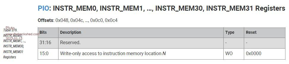 I hope you did not mean these. Write-only access to instruction memory location N. I have tried to read, but all I get is 0. I did not find any other locations.  |
||||
disco4now Guru Joined: 18/12/2014 Location: AustraliaPosts: 844 |
Hi @volhout, A solution to your problem with FIFO being full at program restart might be here. The FJOIN_RX and FJOIN_TX bits in the PINCTRL register description below. When 1, RX FIFO steals the TX FIFO�s storage, and becomes twice as deep. TX FIFO is disabled as a result (always reads as both full and empty). FIFOs are flushed when this bit is changed. Putting a POKE to set the bit and another to clear it at the start of the program should have the affect of clearing the FIFOs PS. This tutorial has been really good. Thanks! Gerry Edited 2023-01-13 07:44 by disco4now Latest F4 Latest H7 |
||||
| Volhout Guru Joined: 05/03/2018 Location: NetherlandsPosts: 3555 |
@pluto, i didn't see they where RO. Sorry @disco4now: good find, peter may use that to clear them. Volhout PicomiteVGA PETSCII ROBOTS |
||||
| phil99 Guru Joined: 11/02/2018 Location: AustraliaPosts: 1793 |
Something like this for PIO 1,0 ? addr% = &H50300000 + &H0D0 POKE BYTE addr%, 1 POKE BYTE addr%, 0 |
||||
