
|
|
Forum Index : Electronics : 150V 45A MPPT - roll your own
| Author | Message | ||||
| poida Guru Joined: 02/02/2017 Location: AustraliaPosts: 1432 |
Thanks Mark. I think I will be right for most things. Still nothing delivered yet... wronger than a phone book full of wrong phone numbers |
||||
| poida Guru Joined: 02/02/2017 Location: AustraliaPosts: 1432 |
Evidently RS-Components have issues of stock movement due to COVID19 So NO nice big-ass diodes or 150V MOSFETS for poida. I do have some HY5110 MOSFETs, 32 in fact. These are 100V equivalents of HY4008. But I need diodes too. Ahh, I can use the body diode of the MOSFET. specs of HY5110 say Trr is about 74ns which is not too shabby for something that does not call itself a Shottky diode. The body diode is good for 316A continuous current. Good luck taking the heat away from that situation. And Vf is 0.8V So I will build one PCB using 4 HY5110, 2 as MOSFETs, 2 as diodes. The diode MOSFETs will need their gates tied to Source. Well, why not? The preferred TO-247 30A 30CPQ080 diodes are not going to arrive anytime soon. All I loose is a bit faster Trr and about 1/2 Vf. It will be good enough to develop the code I reckon. Any dissenting views? What am I missing here? wronger than a phone book full of wrong phone numbers |
||||
| poida Guru Joined: 02/02/2017 Location: AustraliaPosts: 1432 |
Further to using the body diode of a MOSFET as the diode in a buck converter, I did a test. Vin 25V Vout 12V The diode is a F20LC30. Trr is 30ns, 300V, 30A. Vf is 1.3V at 10A This is one I picked out of the salvaged parts box. The HY4008 body diode has a Trr of 30ns and Vf of 0.8 I in I out P in P out effic (HY4008) 0.55 1.00 13.75 12.00 0.87 1.05 2.00 26.25 24.00 0.91 1.56 3.00 39.00 36.00 0.92 2.06 4.03 51.50 48.36 0.94 2.59 4.98 64.75 59.76 0.92 (F20LC30) 0.55 1.00 13.75 12.00 0.87 1.06 2.00 26.50 24.00 0.91 1.57 3.00 39.25 36.00 0.92 2.10 3.99 52.50 47.88 0.91 2.63 5.00 65.75 60.00 0.91 results show using the HY4008 results in better efficiency. I would have been happy to loose a bit to be honest. My guess as to why it's better is thanks to the lower Vf or forward voltage drop of the HY4008 diode. So this is good news, I can build a decent test mppt controller using HY4008 or HY5110 as a diode. I am quite aware of synchronous buck converters, where the diode is replaced with a MOSFET switch. I have used the MOSFET in the above tests with the gate pin tied to Source (pin 3) to ensure the MOSEFT never switches on. To build a synchronous buck converter you will need gate drive signals for both the main MOSFET switch as well as the rectifier switch. The signals are just like 1/2 of an inverter, with dead time. One gate drive has to be isolated from ground and the other (rectifier) is referenced to ground. Just like 1/2 of an inverter. Synchronous buck converters are usually more efficient. The Morningstar MPPT controller is of this type. The efficiency comes from having instead of large currents passing through a diode, it now passes through a fully switched on MOSFET. At 10A (say) and Vf of 1.0V, a diode will consume 10W. Rds(on) for the HY4008 is 2.9mOhm so power consumed by that when passing 10A is 10 x 10 x 2.9e-3 W = 0.29W. No wonder buck converters nowadays are frequently synchronous rectifier types. according to http://www.ti.com/lit/an/slva477b/slva477b.pdf, the diode/MOSFET will see a current of I(out) * (1 - D) where D = duty cycle. Let that = 0.5 for now. So the diode will see 45A x 0.5 or about 23 A average. What diode loss could I expect and what loss when I use a MOSFET to switch like a diode? Diode Vf = 1V, 23A current so power loss is 23W just with the diode. MOSFET Rds(on) = 2.9mOhm so for 23A it's 1.5W My 45A, 54V output is 2,430W. I expect about 90-92% efficiency so 194 to 240W will be lost as heat at full power. Going synchronous will get me to about 95%. This is 121 W lost as heat. 70W to 120W more going into the battery at full power is not a lot, 3-5% actually, but it brings added complexity to the charge controller design. I do not expect to see this sort of power often but when it occurs I want the charge controller to just survive - it will make a good amount of heat - but keep on keeping on. Edited 2020-04-04 14:23 by poida wronger than a phone book full of wrong phone numbers |
||||
| poida Guru Joined: 02/02/2017 Location: AustraliaPosts: 1432 |
And I just made a synchronous buck converter. A HY4008 as switch and another HY4008 as rectifier. 25V in 12.0V out (same 20kHz PWM, 47uH inductor) Results: I in I out P in P out effic difference (W) 0.59 1.04 14.75 12.48 0.85 2.27 1.05 2.00 26.25 24.00 0.91 2.25 1.53 3.01 38.25 36.12 0.94 2.13 2.01 3.99 50.25 47.88 0.95 2.37 2.50 5.00 62.50 60.00 0.96 2.50 The losses are independent of the output load, nearly. And it was easy to get 0.95 or more efficient wronger than a phone book full of wrong phone numbers |
||||
renewableMark Guru Joined: 09/12/2017 Location: AustraliaPosts: 1678 |
Nice work mate 95% is as good as anyone has got yeah? Cheers Caveman Mark Off grid eastern Melb |
||||
| BenandAmber Guru Joined: 16/02/2019 Location: United StatesPosts: 961 |
If I can help in any way please let me know I have a lot of parts here When buying parts in the past I would buy the kit that had the parts I needed I can take a few pictures and upload them I have lots of different components Or if there's components I can get here in us and sent to you that would be great also any way I can help!!! Edited 2020-04-05 10:26 by BenandAmber be warned i am good parrot but Dumber than a box of rocks |
||||
| Warpspeed Guru Joined: 09/08/2007 Location: AustraliaPosts: 4406 |
Its really really tough to do any better than that. Going from 95% to 97.5% would require the total losses to be halved. Not going to be possible. Its an excellent result. Cheers, �Tony. |
||||
| poida Guru Joined: 02/02/2017 Location: AustraliaPosts: 1432 |
This 95% is only in testing, with low loads. I think I will settle on a design that uses diodes for the rectifier function. It will limit the efficiency to some extent, not too bad in my view. I believe if I used a synchronous rectifier design I will eventually come to the point where the buck converter is suddenly working backwards, to become in actual fact a BOOST converter, taking the battery voltage and boosting it up to huge voltages, to be then put through the various things connected to the input terminals. I don't want that to happen. Sure, with good code and enough sensed inputs I might be able to avoid it, but it will never happen if I use diodes. And never having a bad thing happen is high on the list for the this MPPT controller. reading the attached file 8244.Ringing Reduction Techniques for NexFET high performance mosfets.pdf.zip shows an unknown failure mode (to me) and I want to protect the controller from this. This article is well worth a read, give it some time maybe, we seem to have a bit nowadays. The failure mode is when the main switch turns ON, pulling the cathode of the diode up to Vin and pumping current into the inductor. There is a likelihood of some large amplitude ringing of this point in the circuit. This point (A in the below diagram) is the Source of the MOSFET. Sometimes the voltages of this ringing can exceed the MOSFET Vds rating. 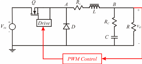 The ringing is related to the diode reverse recovery process. I am firming in my view that our home built inverters blow up due to short period over voltage situations on the Gate or Drain-Source. Hardly ever over current. Sometimes over temperature.. So I am obsessed now with over specification voltages applied to MOSFETS. Below is the result of testing 3 situations, changing one thing only. #1 is no ferrite bead on the Source pin of the MOSFET #2 has a large ferrite bead #3 has a rather smaller bead I show the voltage at point A when running at 5A, 12V output with 30V input. First is no ferrite bead. 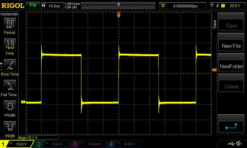 and closer in time, showing the large amplitude ringing 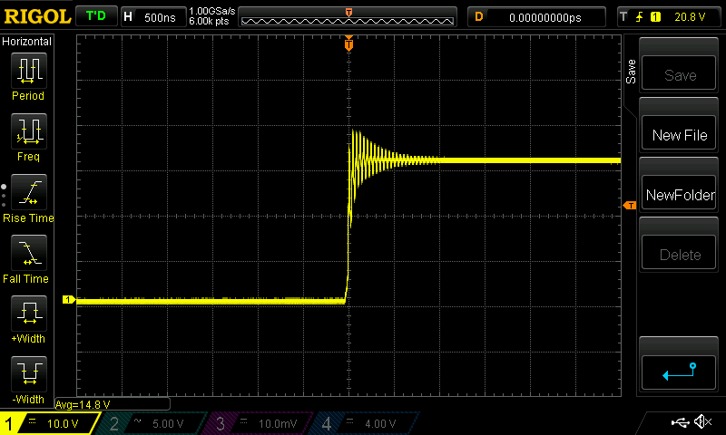 now with the large ferrite bead  no ringing at all 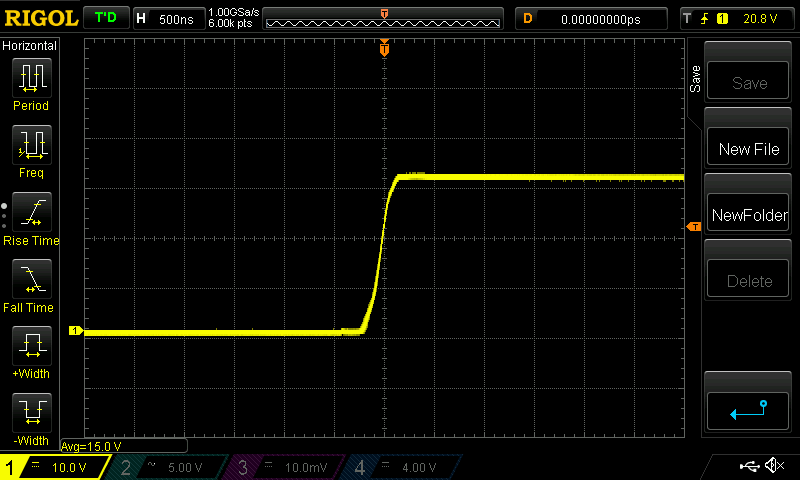 and the much smaller bead 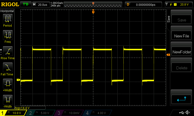 close up 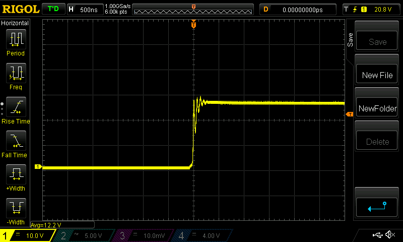 I found that the amplitude of the ringing was proportional to the output current. I wonder how big it would get when driving a 45A output? This is what the point of this post is all about. I did a check on efficiency for the 3 test cases and using a synchronous rectifier. Let's see how much we might stand to loose. 25V In, 15V at 5A out. 75W output I use now 1/2 of the power board out of a Powerjack inverter, one HY4008 on the high side, 1 HY4008 on the low side. I have a simple switch that prevents gate drive on the low side MOSFET, giving me either a diode or a synchronous rectifier simply by switching the drive on or off. HY4008 as a diode no bead : 3.18A or 79.5W in, 94.3% large bead: 3.13A or 78.25W, 95.8% small bead: 3.16A or 79W, 94.9% HY4008 as a synch rectifier: No bead: 3.15A or 78.75W, 95.2% This is very good efficiency Clearly in this test, there is no need to use a synch rectifier in place of the diode. I am firming in the choice of having these large ferrite beads on the Source pins of the MOSFET in the charge controller. Once the PCBs arrive I can test this idea in a larger power situation. Maybe the ringing will appear with much larger currents and voltages? I planned on using OnSemi's FDH055N15A and the IRFP4321 in the two controllers I will build. These are rated at 150V. With an input of 110V, only 40V of ringing might be enough to over volt them. Maybe the ferrite bead will be enough. wronger than a phone book full of wrong phone numbers |
||||
| poida Guru Joined: 02/02/2017 Location: AustraliaPosts: 1432 |
Warp, there is a US patent that describes what Morningstar do in their MPPT controllers. Search for US patent 8513913. They work to get a couple more percent out of the synchronous design and get it. It's about reducing the losses in the rectifier body diode I think. It's hard to read the patent though. wronger than a phone book full of wrong phone numbers |
||||
| Warpspeed Guru Joined: 09/08/2007 Location: AustraliaPosts: 4406 |
There are quite a few ingenious schemes for super efficient power conversion around, but are often not easy to implement in a design that has very different requirements from the demonstrated example. I agree that active rectifiers can be bad news when combined with a battery load, it opens up a whole nest of potential horrors. The problem with conduction losses is that the losses increases at a rate of current squared. A higher voltage system may help a bit, but buck regulators are usually at their very best efficiency when the input and output voltages are fairly close, especially at full load. If you can run it up to near 100% duty cycle, diode losses become negligible, as does ripple current. If stepping down from 150v to 50v, peak current will be rather high in the switching device, which is going to be off most of the time, and the lossy diode will be working overtime. I might be tempted to suggest multiple smaller buck regulators operating in parallel using single devices. Much safer to build five ten amp buck regulators than try to parallel up five mosfets in one monster buck regulator. The current is forced to share equally between devices, the heat spreads more evenly too. The magnetics will be easier to design and fabricate as well. Cheers, �Tony. |
||||
| nickskethisniks Guru Joined: 17/10/2017 Location: BelgiumPosts: 462 |
That's why I have chosen for a simple diode in my design, but I only convert 60-65V to 50-56V. So working duty is low for the diodes. Working perfectly, I like your scope images, the ferrites is something I didn't test. If I make extra spare boards, that will be something I would test and consider. Do you have a link/refference to those beads? I can allways sent you a few 100V diodes for free, the ones I used in my design. That's something small I can do for all the hard work you share here. But I'm not totally convinced they would last in a 150V setup. In theory there are 150V pulses on the kathode of the diode, no? |
||||
| wiseguy Guru Joined: 21/06/2018 Location: AustraliaPosts: 1206 |
I also agree that the complexity of proper gate drive for the lower synchronous Mosfet when used with battery charging does not justify the modest increase in the efficiency for the MPPT proposed. A switching mistake could have undesired or even catastrophic results as Poida rightly points out. With regard to source inductance, in my experience, inductance in the source circuit for fast switching is something to avoid rather than implement. �I do not argue that the ringing appears to have been "cured" in the CRO shots, but the switching times would have also been slowed usually leading to less efficiency (& ringing). I am uploading another discussion paper about source inductance and its effect to compare with the page that Poida pointed to. It is here: SourceInductanceEffects-1.pdf Skipping over the arduous text, below is point 5 in the conclusions: 5. Given all of the above, improvements in gate-drain charge, Qgd, alone will not result in any significant improvements in switching times if the source inductance is large enough to adversely affect the rise and fall times. In order to take full advantage of the improvements in Qgd we must have: - PCB layout with minimum trace inductance - MOSFET package with minimum source inductance Admittedly this is all more of a problem when using a synchronous lower FET instead of a diode. � My suggestions for avoiding ringing is to try to add inductance to the diode leg if using the FET as a diode (lets refer to it as a MOSdiode?) put the ferrite bead on the Drain, try snubbing across the lower diode (or MOSdiode) Lastly try adding a ferrite bead on the drain of the upper MOSFet. Lastly whilst fast switching usually has higher efficiency, their can be a downside, the very fast rise/fall times of the switching edges can have harmonics from DC to light (almost) and can induce oscillations into any current carrying conductor. The oscillations are not always semiconductor misbehaviour or instability per se although the circuit oscillations can cause undesired and dire consequences to the switching device. I am not trying to point score - I also want the most reliable unit we can manage whilst ensuring that when we add parts they are put in the best places for the best effect. If that proves to be the Source it goes against most of my experience & understanding. Poida I do have some BYV32-200 T0220 devices - would you like a few to try out they have a relatively low VF are bloody fast 35nS but only 16A - would need a couple in parallel. Edited 2020-04-05 19:54 by wiseguy If at first you dont succeed, I suggest you avoid sky diving.... Cheers Mike |
||||
| poida Guru Joined: 02/02/2017 Location: AustraliaPosts: 1432 |
Let's see what the average current through the diode will be. Most sources state the diode's I(ave) = (1-D)*I(out). One source for this equation is here The charge controller's specs are 45A output, 90 - 100 V in, 55V out, 2475W output The duty cycle is Vout/Vin so D = 0.5 approx. I(ave) = (1-0.5) * 45 = 23 A Using the HY4008 body diode, we have a Vf of 0.8V at 100A, with the gate tied to the source. The power loss of a diode (ignoring all but DC conduction losses) is due to the voltage drop, Vf. The power loss from the 23A average current will be 23V x 0.8A = 18 Watts Where am I making mistakes? The diode does not see only DC, there are current peaks and even then, the diode will still dissipate heat from the Vf x current relationship. Which has no square or cubed terms in it. Ignore also Vf dependency on temperature for now. We can go hard and determine the RMS current if you like but the resulting number will still be so small as to be insignificant in my view. My specs for the controller are to take a nominal 100V input and drive a 48V lead acid battery. This is what I need. Here is last Friday's voltages of the 100V 3kW array and the battery. Light Blue is the array voltage (i.e. the buck converter's Input voltage). Green/Blue is the battery or the converter's output voltage. 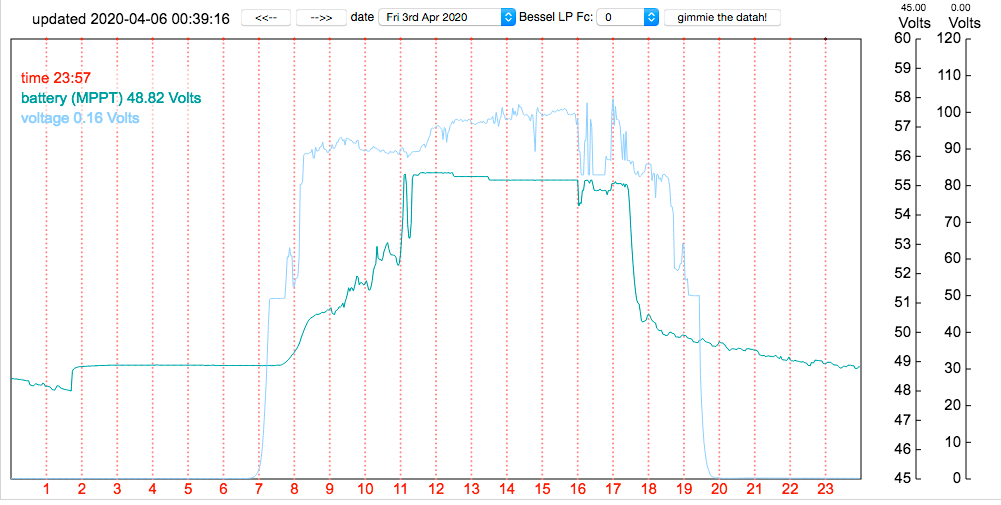 I do not want to venture into 150V DC inputs, for one thing, I am not a qualified electrician and so playing with 150V DC is not on the agenda. nickskethisniks: The large ferrite bead is one of a few I got from RenewableMark. He bought them from Jaycar, a local AUS parts store. I have no idea what part it is. Sometime back I tested the inductance and it was quite large. Again, no idea of the material. Wiseguy: thanks for the offer of the BYV32-200. I have about 10 still servicable HY4008 removed from dead inverters. One of these will be enough for testing. I think I will fit 2 on a prototype controller PCB. And then what about current sharing with diodes? I think it's going to work out fine using the HY4008. I will test beads on the diode cathode leg. Maybe tomorrow. The beads are to be used to protect the MOSFETs from over voltage. I do not care if it costs a little power or makes a little heat. A final note: Eventually the PCBs will arrive and then I build one using the HY5110 100V MOSFETS. This will be enough voltage headroom to do some high power testing. The required 150V MOSFETS are awaiting air freight from UK to AUS. COVID19 will probably prevent me getting them for months. Edited 2020-04-06 01:50 by poida wronger than a phone book full of wrong phone numbers |
||||
| Warpspeed Guru Joined: 09/08/2007 Location: AustraliaPosts: 4406 |
https://pdf1.alldatasheet.com/datasheet-pdf/view/1146879/HUAYI/HY5110A.html I think it would require some caution about the max dc input voltage never exceeding the 100v limit. But otherwise a rather nice device. We may need to think about having minimal loading on the solar panels after the battery is fully charged in a clear blue sky, and cloud edge effect momentarily creating some abnormally high high dc voltages. We might be looking at a system using strings of two 24v panels in series, with max rated open circuit voltage about 42v to 45v per panel, and peak power voltage around 30v per panel. At full power it would be converting 60v solar to charge a 48v nominal battery, possibly at up to 56v. That could be made to work very efficiently. A system with strings of three series connected 24v panels will easily exceed the 100v maximum rating of the mosfets under no load conditions. The estimated diode operating conditions sound pretty right to me, and diode power dissipation should be almost proportional to dc output current. Edited 2020-04-06 07:54 by Warpspeed Cheers, �Tony. |
||||
| poida Guru Joined: 02/02/2017 Location: AustraliaPosts: 1432 |
I value highly your contribution to this topic Warp, Mike and everyone, there are some potential problems in the design and use of the charge controller that I want closely examined and any of my approaches need to be questioned. There must be some sort of design review process. Firstly, since I can not get the 150V MOSFETs yet, I will build a test CC using what I have at hand, which are 32 x HY5110. These are only 100V and not what I will use in a completed CC. But it's lucky they are 100V since they will be exposed to potential destructive conditions under lower input voltages so I can see and test things with lower voltages. Design review: I foresee the CC (charge controller) will have inputs of Volts IN, Volts OUT, Current IN, Current OUT, heatsink temp, inductor TEMP. The 2 voltage sense inputs are across the input and filter cap banks respectively so they change slowly. I want to protect the CC from Vin > design max, Vout > design max, Iout > design max, over temp of heatsink and inductor, etc. The CC firmware will stop PWM when any limits are approached. Firstly, Vin > design max: Commercial CC have the capacity to disconnect either the input and/or the output when the input or the output voltages are exceeded. I suspect this is done by a series MOSFET, between Vin terminals and bulk caps, and another series MOSFET between Vout terminals and output filter caps. I doubt a relay is used since the high DC current will weld the contacts together. Looking at 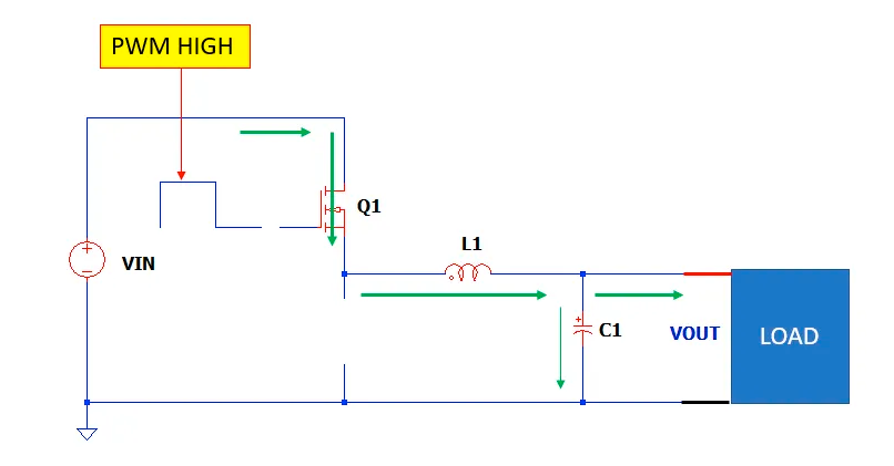 it shows the current path when the MOSFET is switched ON. I then choose to switch OFF the MOSFET and leave it OFF due to Vin > design max. I think we will eventually see the MOSFET Vds become (Vin - Vout) as a maximum value. If Vin = 100V, Vout = 50V, Vds = 50V and so all is OK for a 100V MOSFET. If Vin = 150V, Vds now is 100V and so needs some disconnect protection for the 100V device. The disconnect process will occur under low current, because the CC firmware will have already stopped PWM. I think a series MOSFET is ideal for this and place it on the Vin DC negative input to permit CC DC ground relative gate drive. Maybe an IRF200P222 N channel, 200V, 180A, Rds(on) 6.6mohms. We will have 45A max input when Vin is close to Vout so power dissipated is I2R = 45 x 45 x 6.6 E-3 = 13W. If Vin is normally 100V, then the input current is 1/2 that, and the power is now 1/4 of 13W. $11 from Mouser This all sounds quite easy. What happens when we first connect Vin, maybe it has 100V on it and 60A (a huge solar array), and discharged input caps? Quite large current transients. Damaging transients? So we need to protect the protection device? (a series 10W 33R resistor and small MOSFET for a capacitor pre-charge) Firmware will OPEN the protection MOSFET when Vin is "low or zero" and when > design max. Maybe implement the precharge via a user push button. This will be the CC "ON" button. Once the caps are charged enough, the firmware then switches the protection MOSFET to ON and starts the main program to charge the battery. Once the Vin protection is sorted I want to look at Vout protection. wronger than a phone book full of wrong phone numbers |
||||
| Warpspeed Guru Joined: 09/08/2007 Location: AustraliaPosts: 4406 |
Unfortunately that is not true. It is certainly like that until the mosfet turns on for the very first time and puts some stored energy into the choke. When the mosfet subsequently turns off, the stored energy in the choke causes the flywheel diode to conduct. When that happens, the voltage at the junction of the diode and the mosfet source, gets pulled down to something like minus one volt, or one diode drop below ground. There may then be about 101 theoretical volts between the mosfet source and drain. So the mosfet absolutely must be rated for the full max dc input volts plus some suitable extra safety margin. That then becomes pretty limiting as to the choice of suitable reasonable cost mosfets. Edited 2020-04-06 12:10 by Warpspeed Cheers, �Tony. |
||||
| Solar Mike Guru Joined: 08/02/2015 Location: New ZealandPosts: 1162 |
Hi Poida, many of the top higher end mppt controllers use a relay as the disconnect between the PV panels and the battery bank, I would not recommend using a mosfet combination here due to the susceptibility of shorting out on high voltage spikes (eg lightning surges). If you look at my posts for an Experimental Multiphase Mppt controller Here, near the end of Page2 are the PDF schematics, showing how I have implemented this feature. 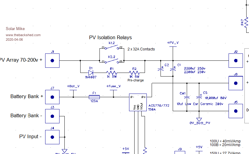 Essentially the high current relay contacts have in parallel a couple of resistors that enable slow charging of the main caps, after the CPU has detected high enough voltage on these the relay is closed (no huge current surge) then mppt starts with gradual duty cycle increase. For disconnect eg at night, the mppt duty is set to nothing and the relay opened. The relay is never used to disconnect with power through it, would require an expensive vacuum relay for this purpose. Cheers Mike |
||||
| poida Guru Joined: 02/02/2017 Location: AustraliaPosts: 1432 |
Thanks Mike for the clue. What happens when the PV array supplies more than design voltage? wronger than a phone book full of wrong phone numbers |
||||
| poida Guru Joined: 02/02/2017 Location: AustraliaPosts: 1432 |
nickskethisniks: the large ferrite bead is 7.8mm outside diameter x 3.1mm inside diameter x 4.8mm high. Inductance is 214uH with 3 turns. Here is how I tested it using the BK precision 879B LCR meter at 10kHz. 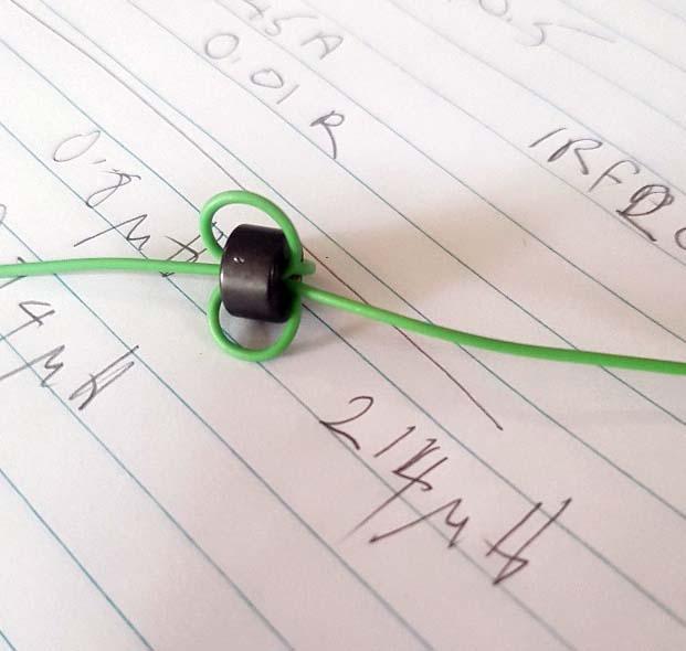 When I test it like this 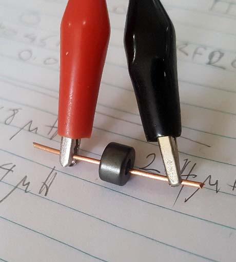 I get 10.8uH at 10kHz I hope this helps. wronger than a phone book full of wrong phone numbers |
||||
| Solar Mike Guru Joined: 08/02/2015 Location: New ZealandPosts: 1162 |
I use a TVS diodes on the input PV to limit any voltages (by shorting out and blowing input fuse) that would exceed the max design spec, eg bulk caps may be 80v, 100v, 160v 200v, 250v etc, mosfets common max = 80, 100, 150, 200, 250 volts. You want to use devices with a min of 20% voltage margin over expected limits for reliability. It is always better with a new design to get it running at a lower voltage, then measure the various higher voltage spikes etc, add additional RC suppression if required, then scale these spikes up for the final working voltage, so you then know what mosfets spec to use for long term reliability. Mike |
||||
| The Back Shed's forum code is written, and hosted, in Australia. | © JAQ Software 2025 |
