
|
|
Forum Index : Electronics : 150V 45A MPPT - roll your own
| Author | Message | ||||
| poida Guru Joined: 02/02/2017 Location: AustraliaPosts: 1389 |
ta, Mike. I have found a nice solution for surpression of oscillation. All tests with 5A output at 15V, 30V in. Dark Blue is gate drive for the switch, Yellow is voltage at the I tried a large bead on the MOSFET switch drain, nothing on diode. 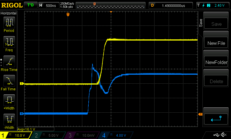 no bead on the switch, nothing on the diode. 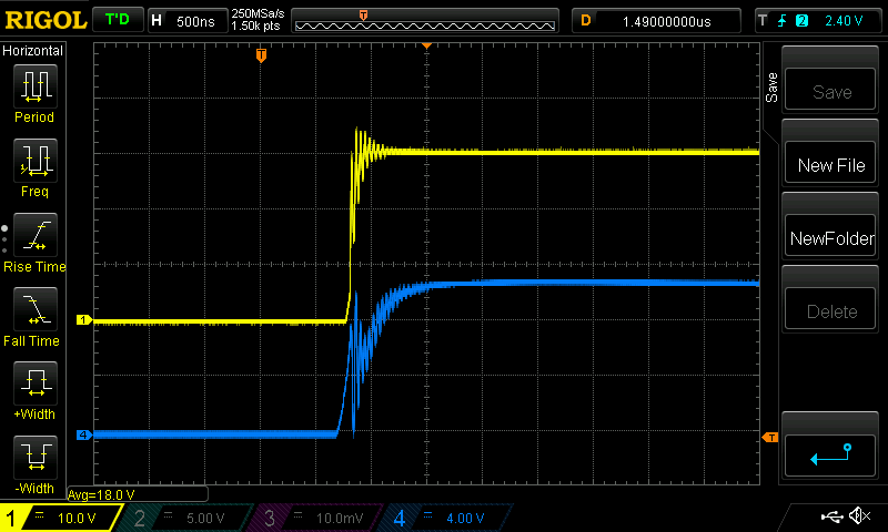 no bead on switch and a synchronous rectifier instead of diode. 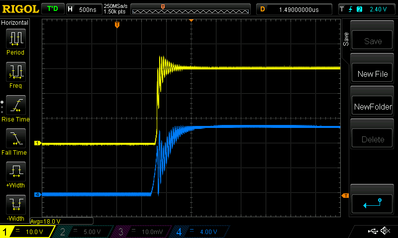 no bead on switch, a small bead on cathode of diode (as suggested by Wiseguy. Mike, please check if this is so?) It seems to help a bit... 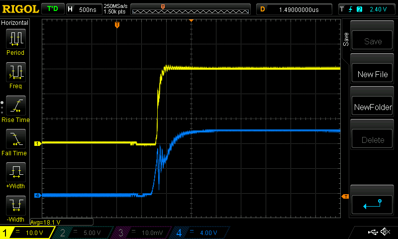 finally, no bead on switch, a small bead on the diode ANODE or source pin. 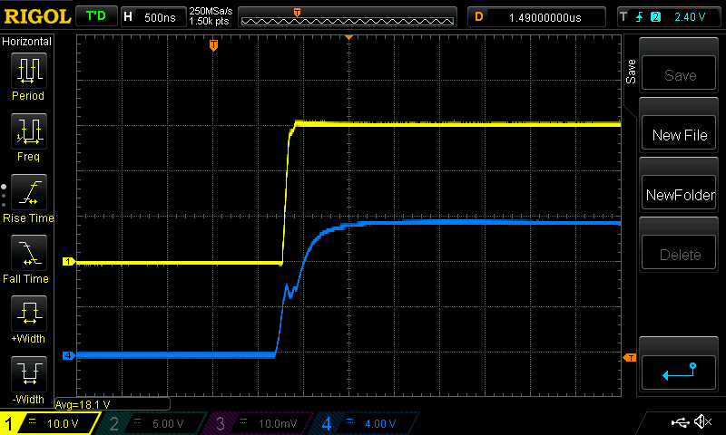 This last configuration is the best I have seen so far. How will it go when the current levels are 10x ? That is the question now. I tried a synchronous rectifier with the bead on the (now) MOSFET source pin and it looks nearly as good. 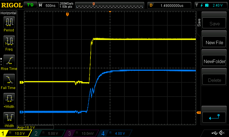 Efficiency: no bead 92.9% bead on anode 92.3% sync rect plus source bead 94.3% nickskethisniks: the small bead is again of unknown provenience. LCR meter at 10kHz with short thick copper wire as in last photo has it at 0.67uH - 0.42uH (offset of the test leads) 5 small beads on the wire take it to 1.72uH - 0.42 offset or about 0.26uH And with this I find it now Beer O'Clock. Edited 2020-04-06 14:33 by poida wronger than a phone book full of wrong phone numbers |
||||
renewableMark Guru Joined: 09/12/2017 Location: AustraliaPosts: 1678 |
these are the large beads Cheers Caveman Mark Off grid eastern Melb |
||||
| poida Guru Joined: 02/02/2017 Location: AustraliaPosts: 1389 |
thanks Mark. wronger than a phone book full of wrong phone numbers |
||||
| Solar Mike Guru Joined: 08/02/2015 Location: New ZealandPosts: 1126 |
Interesting displays there Poida 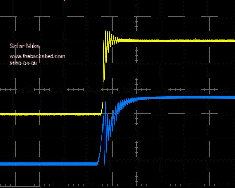 One has to ask, is it the drain oscillations feeding back into the gate via miller capacitance or the gate parasitic's causing oscillation and thus affecting the drain output. You could measure that nice high freq oscillation and use an RC snubber from the formula in that PDF article to dampen it out. Or see if the gate is causing it by increasing the gate drive resistance by several ohms, I would start at say 2r and increase to 10r in 1r steps, see what happens, if not much change place your bead on the gate drive mosfet pin; and make sure your scope probe earth lead is replaced by a short length of copper wire, its easy to get misleading measurements. Cheers Mike |
||||
| poida Guru Joined: 02/02/2017 Location: AustraliaPosts: 1389 |
I am afraid I am in no way ready to perform further experiments with buck converters for the evening. I have had beer. I am enjoying Walter Lewin's 8.02 physics lectures he produced for MIT Boston 15 years ago. time for some R&R as it were. 10:30pm and need to be up at 6:30am. In a coupla days I will do what you want. When you ask is it Miller capacitance driving things, this is something I have always wondered. There are strong forces at work in a MOSFET when we drive the gate from 0 to 15V in 1us. non-zero capacitance of the 3 pins... a nightmare. And the Vds chage rate induces voltage changes in the gate. And more. As an aside, the above post with 6 DSO captures used identical measurement instrumentation. I altered nothing, even down to avoiding moving the two unsheilded wires going to the differential probe inputs. Common mode interference, etc. is a major worry and I think if I just accept there will be some, then just make one change and compare the difference. This should give me something to think about. The above tests use an IR12844 driver, into 4.7 Ohms. I will change it in 5R steps I think, going 1R at a time is too slow for me. I am well aware of scope earth lead inductance. With zero change in probe lead position, you can see profound changes in the switch/inductor node voltage in the above 6 captures. Probably I will investigate the health of the converter when built on the PCB. Then I will use good probe tech. Now I only want to get a feel for what might be good to build. wronger than a phone book full of wrong phone numbers |
||||
| Solar Mike Guru Joined: 08/02/2015 Location: New ZealandPosts: 1126 |
Good one Poida, beer is definitely required, I'm just about to bottle a 23L brew of Irish Stout. Here is a dia. of how the drain capacitance affects the gate drive, IGBT shown, but same for Mosfet. 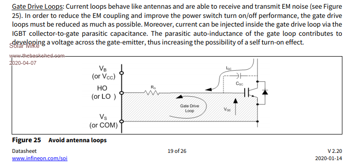 keep the driver 21844 output to 10mm of your mosfet if possible, this reflects a lower impedance across the gate/source and helps prevent the gate voltage rising to turn on levels during any oscillation; Prob not possible without a final pcb design. Cheers Mike |
||||
| poida Guru Joined: 02/02/2017 Location: AustraliaPosts: 1389 |
Solar Mike: I have made a very tight gate drive loop as shown above. Here is my attempt. There is a 10K gate to source pull-down and a 10R gate drive resistor. 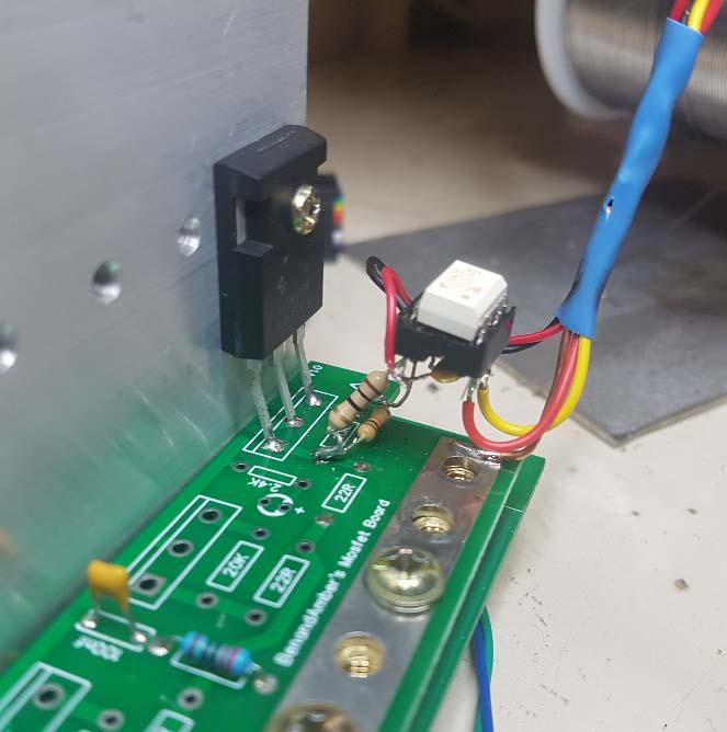 I use the TLP 250 instead, this is what is required on the PCB. I show gate voltage, switch/inductor node and pwm logic drive in Dark Blue, Yellow and Light Blue respectively. Tests were done with zero gate resistance, 4.7R, 10R and the DSO captures are at about 5A output. The rectifier is a MOSFET with gate tied to source via a link. No ferrite beads in the first 3. Zero gate resistance: 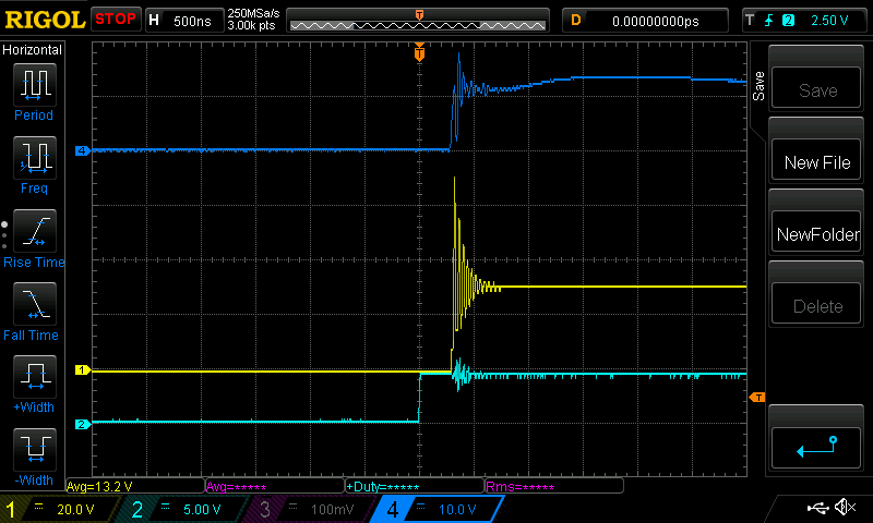 4.7R 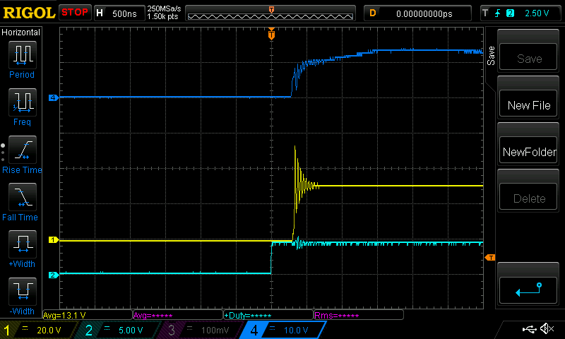 10R 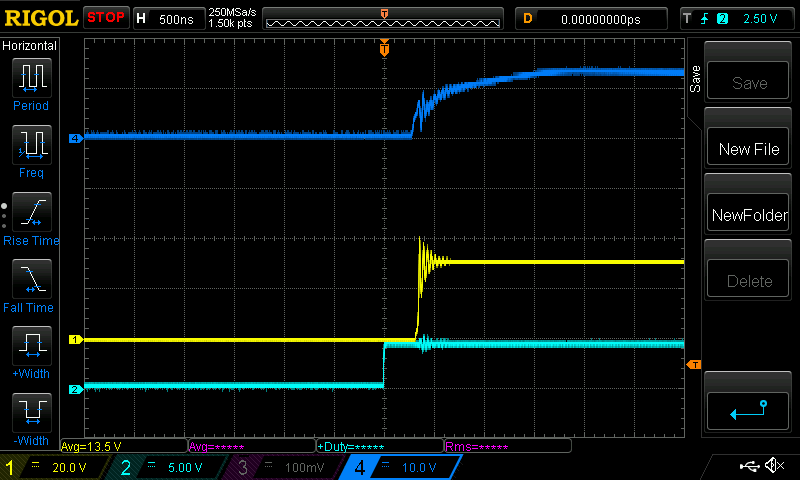 Not real good looking situation, just less of the bad thing. With zero gate R we see voltages in the order of 70V. This voltage also is across the diode. Now I tried the MOSFET diode with the small bead on the source pin with 10R gate R. 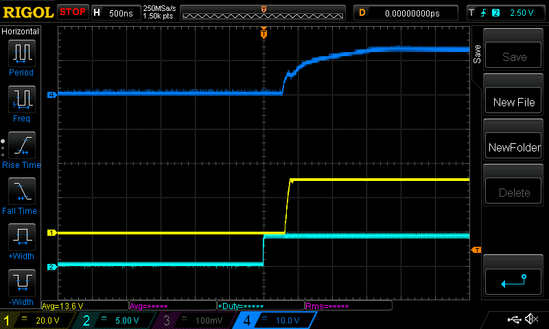 Excellent. The gate of that MOSFET is pulled down with a 20K not a copper link and it permits the MOSFET's diode behavior to be rather softer/slower in it's commutation. The combination of both appears to work well here. But there is oscillation still and it's at the other end of the switch event, when it opens. I wonder how we can reduce this? 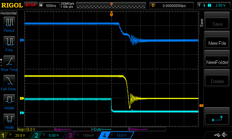 Maybe a bead on one of the pins of the switch? Drain pin is my guess. wronger than a phone book full of wrong phone numbers |
||||
| poida Guru Joined: 02/02/2017 Location: AustraliaPosts: 1389 |
Ok, I put a short across the 20K gate pull down and this is a surprise for me. Using the MOSFET diode with a bead on the source pin. (i.e. the best result) First is the switch ON event, as with the previous post. 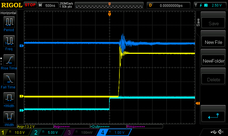 The oscillations are back. and the switch OFF event: 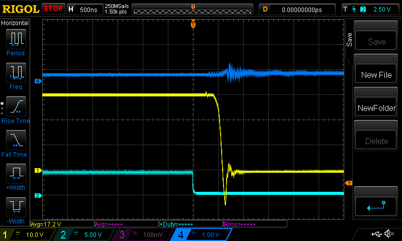 These oscillations are gone! So we can have one or the other sorted out but not both. I now revert to the 20K gate pull down resistor. This gives me some clues. Clearly I need a few. wronger than a phone book full of wrong phone numbers |
||||
| Solar Mike Guru Joined: 08/02/2015 Location: New ZealandPosts: 1126 |
What is consistent is the frequency of the observed ringing, this relates to the wire trace lengths in your circuit. This could be dampened by an RC connected across the rectifier diode to 0v. As you have measured, the amplitude of these are dependent on the speed of the active switching devices, a larger gate resistor 10r slows down the transition and ringing amplitude reduces, however at larger output currents this may be less efficient. 1: I would try the 4.7r gate resistor with a bead over the mosfets gate lead, to dampen that HF oscillation. 2: Under the TLP250 add a 10uf electrolytic parallel with your ceramic cap. 3: Unsolder one end of the gate resistor from the pcb and connect it directly at the mosfet pin, near the case to lessen the inductance path. 4: Also try a 1 amp schottky diode parallel with the 4.7r, anode end towards the mosfet, this will allow a lower impedance path at turn off. Cheers Mike |
||||
| Warpspeed Guru Joined: 09/08/2007 Location: AustraliaPosts: 4406 |
I have been thinking along similar lines to Mike. I would be looking at the supply pin of the TLP250, my bet is that a lot of the ringing might be there as well. A 10uF low esr electrolytic or tantalum may help. And I agree, you cannot have ringing without significant inductance, and that must be damped somehow. A higher series gate resistance should help with that, but at the expense of switching speed. Ferrite beads only work in low impedance circuits. So you get to try either a higher value gate resistor, or alternatively a lower value gate resistor plus one or more ferrite beads in series with the gate. That becomes more complex to get exactly right, but worth it if you need the speed. Beer is good. Cheers, ĀTony. |
||||
| poida Guru Joined: 02/02/2017 Location: AustraliaPosts: 1389 |
Thanks for your input. The way I see it is we see the node voltage drop as soon as the switch goes OFF. For a short while the diode is changing from reverse bias to forward and this takes time. So we have that first and deepest dip in voltage below ground. (this is the test with the MOSFET diode + anode bead + gate to drain short) 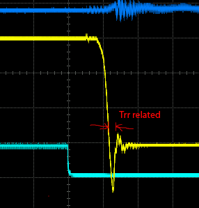 I see the reverse recovery dip as unavoidable when using a diode. Different diodes will have Trr of different values. The HY4008 Trr is 30ns. The width of the dip in the above image is much more than 30ns. Once a large pulse of energy has been inserted into the circuit it comes as no surprise that it wants to ring like a bell. (this is the test with the gate to source resistance = 20K) lots of ringing. I am tending towards the view this ringing is due to the high Q of the circuit and driven by the diode's non-zero Trr. I tried most of your suggestions above. I replaced the 10R with 4R7 gate resistor and put a bead on it. I could not be bothered with a 10uF cap. Let's see if it's gate drive related... Usual test condition, including the MOSFET diode with bead on the anode. 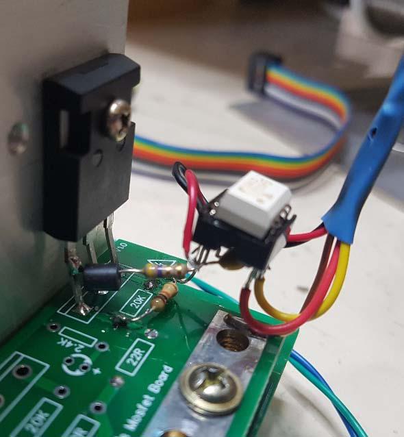 which gave me 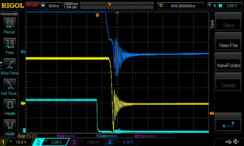 and it looks a bit worse if anything. Not gate drive related because I changed it in a large degree and no significant improvements seen. Is it due to poor probe tech? Here (the Yellow, on the switch/inductor node) I use the small spring ground wire. One slip and I short the diode and likely blow the MOSFET switch. 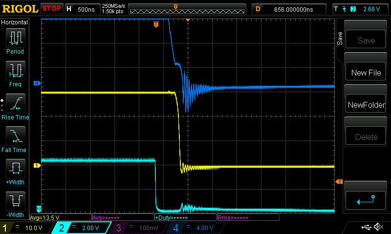 oh no. So I have to repeat it all with good probe technique now? here is the switch ON event with spring ground wire 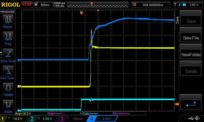 I think I might call it sorted out for now. I have minor voltage spikes and ringing on the switch ON event and again minor ringing and spike in the OFF event. And a surprising amount of EMI upsetting my measurements. I ordered the PCBs from JLCPCB on 28 March and they arrived at Melbourne 2nd April. AusPost has chosen to sit on them since then. Today is 11th April. thanks guys. JLCPCB are good to deal with, they phoned me to check if I got the PCBs and when they saw I did not, they raised a query with AusPost last Thursday without my asking them to do so. That last DSO capture shows a large spike, which is proportional to current, but only present in continuous conduction mode of the buck converter. Time to read some more on the subject. Thanks again for taking some of your time with this. wronger than a phone book full of wrong phone numbers |
||||
| FFTandMe Newbie Joined: 11/10/2019 Location: CanadaPosts: 32 |
Hi Poida, Sorry for being so late to the party. There is a guy on youtube I follow who used a nano to make a much smaller (in terms of capacity) MPPT controller. I dont know if his sketches or schematics would be useful, but here is a link to the vid (his files are in description). https://www.youtube.com/watch?v=5ayqLMxSS54 |
||||
| poida Guru Joined: 02/02/2017 Location: AustraliaPosts: 1389 |
thanks for the info, FFT. It's close to what I want to build so it will give me some hints. Ok, after getting a good probe setup, as seen below: 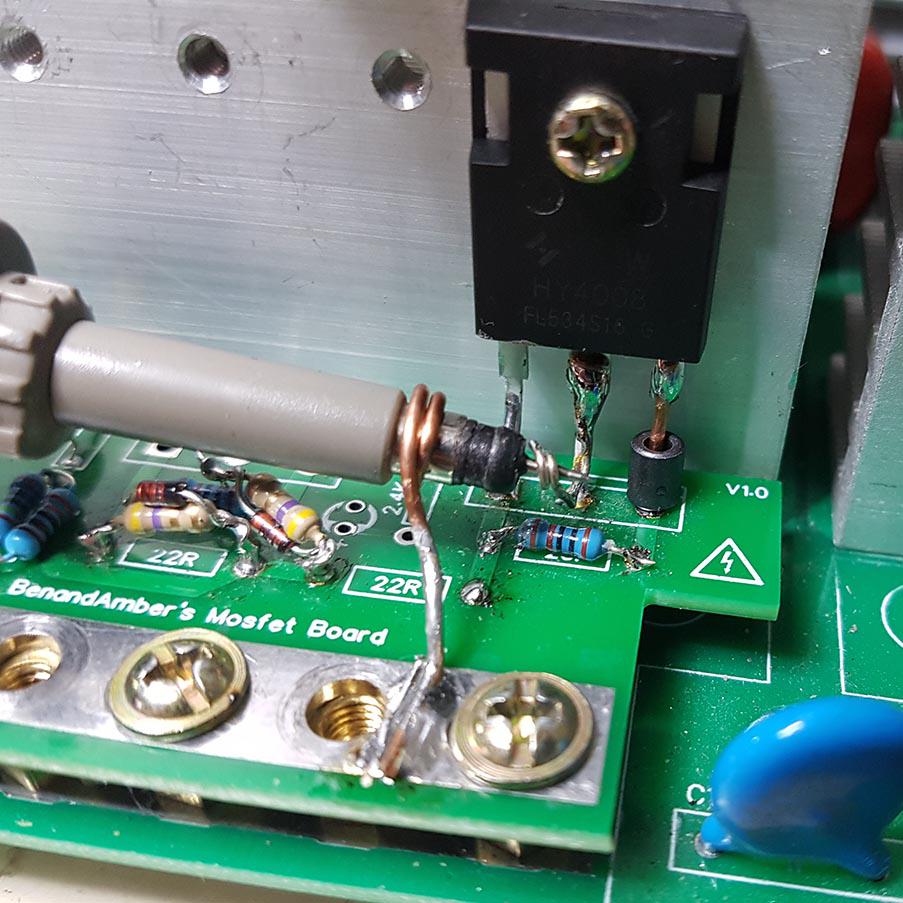 I now get excellent switch ON event voltages 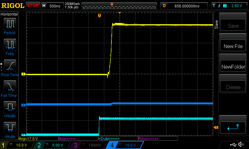 And excellent switch OFF voltages 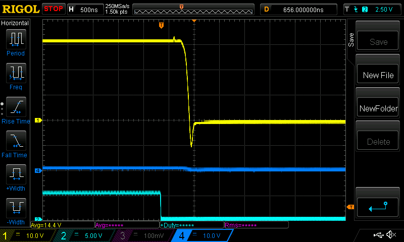 NO ringing anymore. The setup is 10R gate drive resistor. 30V in, 15V @ 5A out A small ferrite bead on the diode's anode (FET's source) pin. Retain the 20K gate to source pulldown resistor, i.e. no short. And a small ferrite bead on the switch source pin. 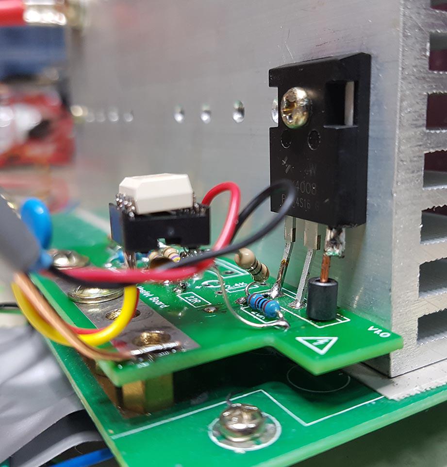 This is as good as I think it will ever be. The RS-Components order has finally arrived so I have now some 150V MOSFETS. The PCBs are lost somewhere in AusPost. Maybe time to reorder and just accept the loss of $100. wronger than a phone book full of wrong phone numbers |
||||
| hugocamaras Newbie Joined: 12/04/2019 Location: BrazilPosts: 24 |
Poida, Yeah... I think it's not just us Brazilians who suffer to receive an international order that arrives very quickly here in Brazil, but that when it arrives, it takes to be delivered to our hands... If it ever comes. the most reliable thing is to make sure that you will not receive your order. Poida, I also follow Homemade 102... Great Channel! This specific project is not his, he just modified it to what he needed... He also said that later on it will increase the working amperage maybe to 40A. I'm waiting for him to do that. |
||||
| renewableMark Guru Joined: 09/12/2017 Location: AustraliaPosts: 1678 |
Sorry to hear the boards didn't show up. They probably will turn up eventually. If you do decide to re order, perhaps add some features to the design. I was thinking it might be nice to have the ability to gang them together, so one controller is the brains for one or more extra units all running together, master and slave type scenario. Another feature could be to use excess power diverted to another source when it's not needed for batteries, ie a hot water heater etc. Maybe an idea for down the track, you probably just want to get something running and proven first. Cheers Caveman Mark Off grid eastern Melb |
||||
| nickskethisniks Guru Joined: 17/10/2017 Location: BelgiumPosts: 418 |
Thank you for the links about the ferrites. Yes, if you order again maybe a few things could be improved. You don't have to use the tlp250, the Fod3182 for example is pin compatible but better for higher frequency and drive current. A question offtopic, I was comparing Eas values of mosfets and the numbers are idiotic high for hy4008 and hy5110 compared to for example irfp4110 or irfp4468. Also the soa curves of those irf mosfets seems silly compared to those chinees mosfets... Anyone tested those numbers? Offtopic again, I'm building a 6fet bldc controller, how much phase current would I set my controller too? I use TO247 mosfets, I can choose between hy4008, irfp4110 or irfp4468 mosfets. I will probably open a topic if I have time. Edited 2020-04-14 20:10 by nickskethisniks |
||||
| Volhout Guru Joined: 05/03/2018 Location: NetherlandsPosts: 3559 |
Hi poida, Although adding a ferrite to the source pin of a power MOSFET may clean up signals there is some risk there. 1/ since the source of the FET silicon is not the same as the ground of the TLP250 (there is an inductor in between), the gate drive may look fast, but actually is slower. The FET needs a fast transition signal between gate and source. Not between gate and ground. 2/ since the TLP250 low impedance output is not connected to the source pin, the MOSFET gate is not driven low impedance (depending the frequency, for DC is will be low). This may result in spurious turn-on of the FET at high dV/dt drain signals (i.e. fast switching). An inductor (or ferrite) in the source (or emitter of a transistor)...that is the way oscillators are made typically. Both may lead to higher losses. I am not trying to change your design, just try to tell you what to look out for. If you see heavy switching losses, or occasionally loose a FET, this may be causing it... Succes with your design... Volhout P.S. I would definitely put a low ESR capacitor between the power and ground pin of the TLP250, as close as possible to the pins. That is just as important as short wires to the FET. Edited 2020-04-15 00:02 by Volhout PicomiteVGA PETSCII ROBOTS |
||||
| wiseguy Guru Joined: 21/06/2018 Location: AustraliaPosts: 1001 |
I have to agree with Volhout about adding inductance in series the source not being ideal engineering practice. ĀAnother factor to consider, in my post about Ferrite beads I showed the voltage spike that the ferrite beads can produce across them at the moment of switch off. ĀI believe the spike I measured was of the order of 30V. Most power Mosfets have a gate max of either +/- 20V or +/-30V. To expand on this the gate source is a microscopically thin layer of oxide that can easily be "punched through" by even a small static charge with essentially no energy behind it. ĀThis spike can damage and might not immediately kill the FET but can be detrimental to its performance and lifetime. ĀThe bead voltage appears between the source and gate at FET switch off. If the inductor is to stay in series with the source, a resistor of 1 - 4.7 Ohms placed in parallel with the inductor would help control (minimise) the amplitude of a spike. ĀAlso a 16 or 18V zener between the Gate and Source is a very cheap insurance add on to protect the FETs gate from damage and has no negative effects that I am aware of. ĀNote if using negative drive a back to back zener should be used. In my experimentation the best results I obtained was by placing the bead on the drain. I have also found when paralleling Mosfets, oscillations can occur that were not evident at all with just one device and that if a small bead is placed on each FETs Gate resistor it has helped eliminate this issue in the past. ĀDriving the Gate hard & fast and minimising the transition time in the miller region can also be helpful in getting rid of these effects. Peter I also ordered PCBs a couple of weeks ago from JLPCB with DHL delivery. The boards are well past their 3 day delivery - this pandemic (and Easter?) has really blown our PCB supply times into the weeds! Also want to add you are using excellent probe techniques - it is the only way to see what is really happening at the pins of the FET. It can be a bit scary I usually make the connection and then apply power and then switch off before removing - one slight slip and its all over lol. Edited 2020-04-15 10:30 by wiseguy If at first you dont succeed, I suggest you avoid sky diving.... Cheers Mike |
||||
| Warpspeed Guru Joined: 09/08/2007 Location: AustraliaPosts: 4406 |
I too am waiting on parts from China that have tracking numbers. Everything must be just sitting in a giant postal warehouse somewhere. Cheers, ĀTony. |
||||
| nickskethisniks Guru Joined: 17/10/2017 Location: BelgiumPosts: 418 |
Don't know why I didn't add an electrolytic cap on my pcb, but on the same place the 100nF ceramic capacitor is you can fit a 10uF ceramic. Then right on top of the 100nF or next to it the 100nF. I think that's ok? |
||||
