
|
|
Forum Index : Microcontroller and PC projects : General purpose I2C IO module
| Page 1 of 6 |
|||||
| Author | Message | ||||
| Mixtel90 Guru Joined: 05/10/2019 Location: United KingdomPosts: 7815 |
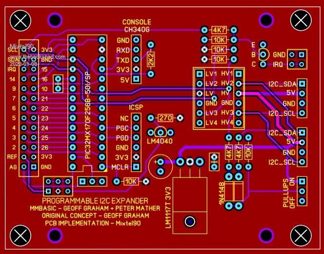 This is designed, with some end panels yet to be sorted out, to fit the 90x70x28 box. I2C connection is looped through so that modules can be cascaded (but addresses will have to be set in firmware). Supply and I2C is at 5V and the SCL and SDA lines are on the outside to reduce cable capacitance. This should allow operation over reasonable distances using ordinary 4-core flat cable. Powering at 5V also allows each board to have its own 3V3 regulator, taking the load off the SMPS on a PicoMite. Note that level shifting is needed if this board is connected to I2C lines that can't handle 5V. However, the 3V3 side I2C lines are available on the IO connector, the pullups are fixed on though. An active high IRQ signal is available on the connector, which drives a cascadable open collector signal back to the host. No pullup is included as that will depend on the host. Pullups on each board can be enabled/disabled from outside the case. Links allow the analogue supply to be external, 3V3 or a 3V reference and the analogue ground can be linked to GND internally. Any further ideas? Mick Zilog Inside! nascom.info for Nascom & Gemini Preliminary MMBasic docs & my PCB designs |
||||
| lizby Guru Joined: 17/05/2016 Location: United StatesPosts: 3347 |
Neat. Noting "ORIGINAL CONCEPT - GEOFF GRAHAM", can you post a link to this (if you mean "concept of MM2 I2C expander" rather than "concept of MMBasic")? Is there proposed or preliminary firmware? PicoMite, Armmite F4, SensorKits, MMBasic Hardware, Games, etc. on fruitoftheshed |
||||
| Mixtel90 Guru Joined: 05/10/2019 Location: United KingdomPosts: 7815 |
All firmware is in the Micromite "Getting Started" manual (page 70 onward), which is where Graham describes this idea. That's why I put "Original concept". :) I've not considered changing anything there, apart from perhaps adding the I2C address as an argument to the host routines so that several boards can be addressed. This is the spec for the above software: Commands on the host: SSETPIN pin,cfg - configures a pin to do something SPIN pin, output - outputs a 1 or 0 value to pin x$ = SPIN(pin) - reads a value from pin cfg can be: 0 Not configured or inactive 1 Analog input 2 Digital input 3 Frequency input 4 Period input 5 Counting input 8 Digital output 9 Open collector digital output. In this mode SPIN() will also return the value on the output pin . Returned values are in the form pf a 12 character string Mick Zilog Inside! nascom.info for Nascom & Gemini Preliminary MMBasic docs & my PCB designs |
||||
| Mixtel90 Guru Joined: 05/10/2019 Location: United KingdomPosts: 7815 |
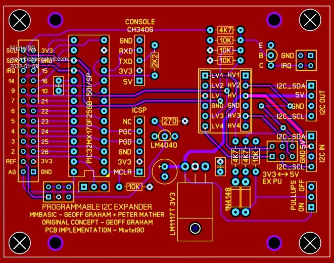 This version *should* be able to be driven directly by a 3V3 system. I2C IN has links to allow either normal 5V connection or spare inputs on the voltage shifter. Outputs from the shifter are paralleled up with the other 5V signals. There are no pullups when a 3V3 system is used as that would apply 3V3 back down the lines to a system that may be powered down. I don't know the circuit of the level shifter so I'm not *certain* about this. Obviously a 5V supply is still required to feed the 5V I2C to the next board. Mick Zilog Inside! nascom.info for Nascom & Gemini Preliminary MMBasic docs & my PCB designs |
||||
| lizby Guru Joined: 17/05/2016 Location: United StatesPosts: 3347 |
Cool idea. I guess I started without reading "Getting Started". PicoMite, Armmite F4, SensorKits, MMBasic Hardware, Games, etc. on fruitoftheshed |
||||
| Mixtel90 Guru Joined: 05/10/2019 Location: United KingdomPosts: 7815 |
I didn't read it either. Now I've discovered that I should have done. :) (Goes off to think about fitting a power LED and if it could do anything else...) EDIT: Found the circuit and it's what I expected. There will be 3V3 on the I2C pins via 10k resistors even if the host is off. Oh well, tough. :) It's probably powering the I2C board(s) anyway so they are probably off too. EDIT 2: Oops! A stray RTC module (well, an option for one) found it's way in. :) Edited 2022-01-09 04:55 by Mixtel90 Mick Zilog Inside! nascom.info for Nascom & Gemini Preliminary MMBasic docs & my PCB designs |
||||
| dMajo Newbie Joined: 18/05/2020 Location: ItalyPosts: 28 |
Funny, I've always thought that the I2C bus capacitance it is not taken in consideration in regards to the cross-talk (the transmission of signals to the adjacent line, through the inter-line capacitance, due to long parallel runs), but instead it have to do with the open-drain nature (as opposed to push-pull) of the bus: being the high level not driven the rise time of the signal increases and the sharpness of the square waves decays being the edges and corners "rounded" thus introducing errors in the bit sampling of the signal. But, anyway the project seems interesting. May I only suggest a P82B715 or a P82B96 in place of your level shifter with a 100nF and a 22uF 25V capacitors on the external bus power supply. These buffers allows up to 12/15V bus levels. And I will reserve the places also for internal-I2C bus pullups on the board. You can always leave them unpopulated. Edited 2022-01-09 05:53 by dMajo ALLdataEE.com EDU Promos |
||||
| Mixtel90 Guru Joined: 05/10/2019 Location: United KingdomPosts: 7815 |
Thanks for your suggestion. I think I'll stay with the level shifter for the moment though, purely on a cost basis as they are very cheap and easy to find. However, I might consider doing another "long range" version later. That would make an interesting project. You can get better performance on I2C using suitably fast constant current sources for the pullups, I believe, but I don't fancy going down that route at the moment either. It's something that could be experimented with. Cross talk between SCL and SDA can be a problem as the clock corrupts the data. It's better to separate them. Cable capacitance is the ultimate distance limiter, so slower speeds work over longer lines and low-capacitance cable is good. You can apparently twist SDA and SCL with their own ground wires or one with ground and the other with supply if the cable has suitably low capacitance. This isn't long range stuff. RS485 is *far* better. I just haven't got round to looking at that yet. :) I was just looking for something quick & dirty to extend the IO of a PicoMite driving a SSD1963 parallel display and got a little sidetracked... EDIT: Oh dear... It's grown a 2-colour LED now. Red for power on, but Green (mixing to yellow) can optionally be connected to pin 14 of the Micromite to put it under user control. Edited 2022-01-09 06:47 by Mixtel90 Mick Zilog Inside! nascom.info for Nascom & Gemini Preliminary MMBasic docs & my PCB designs |
||||
| phil99 Guru Joined: 11/02/2018 Location: AustraliaPosts: 2579 |
"Cross talk between SCL and SDA can be a problem as the clock corrupts the data. It's better to separate them. Cable capacitance is the ultimate distance limiter, so slower speeds work over longer lines and low-capacitance cable is good. You can apparently twist SDA and SCL with their own ground wires or one with ground and the other with supply if the cable has suitably low capacitance." Exactly the same issue and solution with Tx and Rx on TTL serial. |
||||
| Tinine Guru Joined: 30/03/2016 Location: United KingdomPosts: 1646 |
Ah-ha...Good, you brought it up  I didn't want to question this project but I2C is something that I considered a long time ago. I opted to go with 485/422 multi-drop (full-duplex). The master keeps the TX to itself and the RX is a slave-shared response line. I use a binary protocol with a simple checksum. Running constantly @230K Baud (overkill) and never had a checksum error. Environment: Multiple 2KW-5KW PWM-ing servo amplifiers (aka: drives). Full duplex + differential drivers/receivers =  Edited 2022-01-09 21:28 by Tinine |
||||
| Mixtel90 Guru Joined: 05/10/2019 Location: United KingdomPosts: 7815 |
I'm mot envisaging this I2C system to be working over more than a couple of metres really, not much more than an experimenters test bench/demo table. The thing is, it's very cheap and easy to implement and is pure, easy to follow MMBasic stuff. It's intended to work with the SSD1963 converter board that I'm also looking at, which would also have a Micromite on board to give 4+17 IO. This module would give it a further 17 remote IO at very little extra cost. It's also usable with other I2C devices - or it can run completely independently of anything if you just feed it with 5V and change the firmware. I don't think it would be difficult to do a second version of the SSD1963 converter but with RS485 instead of the Micromite and 5V I2C. Just an extra PicoMite pin for half-duplex. (Keeping costs and pcb space down again!). Mick Zilog Inside! nascom.info for Nascom & Gemini Preliminary MMBasic docs & my PCB designs |
||||
| Turbo46 Guru Joined: 24/12/2017 Location: AustraliaPosts: 1638 |
RS485  Checksum  Mick, if you could find room for a MAX485 the board could be more versatile? Just a thought. Bill Keep safe. Live long and prosper. |
||||
| Mixtel90 Guru Joined: 05/10/2019 Location: United KingdomPosts: 7815 |
Won't fit at all in the current configuration, sorry It's designed to go in a specific case so it would have to be 485 OR I2C, but not both. Not only that, but all the firmware would be a rewrite. Perhaps as a later project. I'm sticking with the KISS principal for the moment. :) Remember that the Micromite would be handling the 485 as well as the IO. I would lose a pin for half duplex or a fair bit of board space for full duplex. Current circuit (it's probably about right): 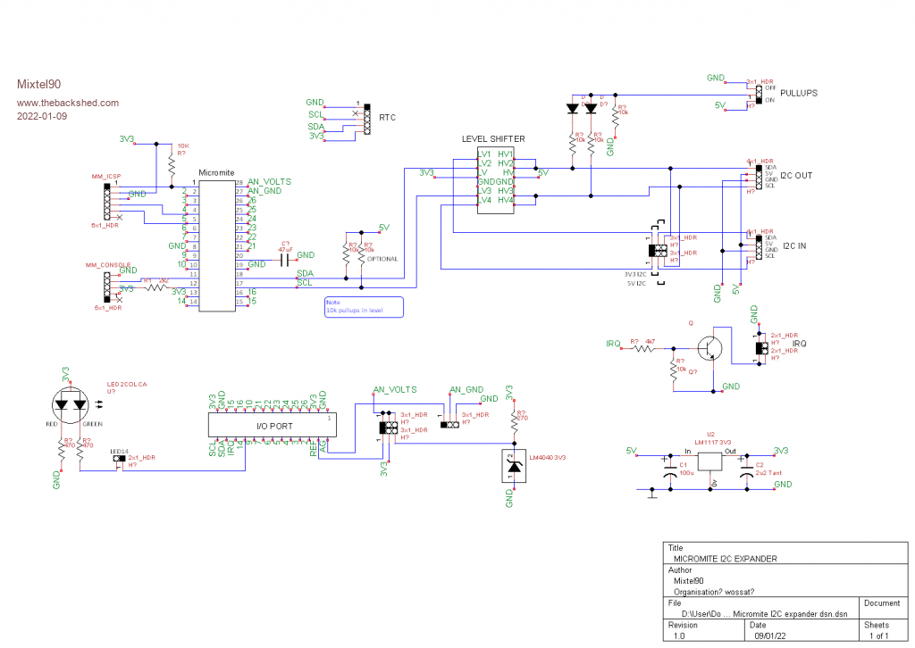 Mick Zilog Inside! nascom.info for Nascom & Gemini Preliminary MMBasic docs & my PCB designs |
||||
| Tinine Guru Joined: 30/03/2016 Location: United KingdomPosts: 1646 |
@Mixtel90 Remember the data-driven enable I posted that you said you liked?  |
||||
| Tinine Guru Joined: 30/03/2016 Location: United KingdomPosts: 1646 |
@Turbo46, Do you see a weakness? The command packets have the following structure: Header byte (always 0xAA) Module Address byte (0 - 255) Command byte (2 nibbles) Additional Data bytes (0 - 15 bytes) Checksum byte (8-bit sum of the Module Address byte through the last additional data byte) The Header byte is used to signal the beginning of a command packet. When waiting for a new command, each module will ignore any incoming data until it sees a Header byte. The Module Address byte is the address of the target module. The Command byte is broken up into an upper nibble (4 bits) and lower nibble (4 bits). The lower nibble contains the command value (0 - 15), and the upper nibble contains the number of additional data bytes required for that command (0 - 15). IOW, the recipient is made aware of the number of bytes to expect. Edited 2022-01-10 00:19 by Tinine |
||||
| Mixtel90 Guru Joined: 05/10/2019 Location: United KingdomPosts: 7815 |
The Micromite has a COM1 DE output that goes low on send to use with the direction input on a 485 transceiver - pity it's inverted... Oh yeah... I remember seeing that... I can do you a pcb for a 485 version if you want to have a play. You could link two together. :) You'd have to sort out the firmware for both ends though 'cos I'm having far too much fum playing with pcb design. :) I'd suggest a simplified firmware though. It doesn't need to be very flexible and could use the same SSETPIN, SPIN and SPIN() approach to keep things simple for the user. After all, it's only controlling a Micromite. Edited 2022-01-10 00:48 by Mixtel90 Mick Zilog Inside! nascom.info for Nascom & Gemini Preliminary MMBasic docs & my PCB designs |
||||
| Tinine Guru Joined: 30/03/2016 Location: United KingdomPosts: 1646 |
Cheers but I already have the full-duplex system. It's how my Explore E-100s talk to my motion control chips. I have a whole bunch of MAX491s |
||||
| Mixtel90 Guru Joined: 05/10/2019 Location: United KingdomPosts: 7815 |
Oh well... :) Here's an RS485 half-duplex version anyway. I *think* it might work. It has the same number of usable IO pins, but the I2C pins 17/18 replace 21/22 which are needed for COM1. Can't do a loopthrough if I use a DB9 as the box isn't big enough. :) 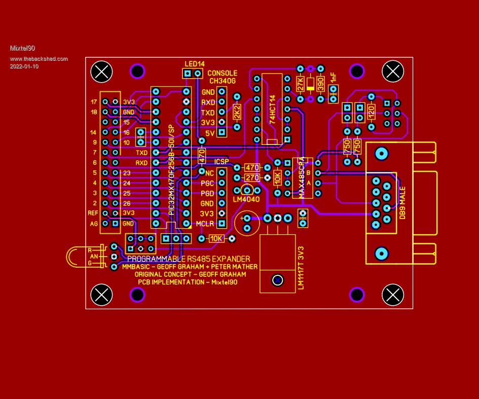 And just for completeness, here's the circuit: 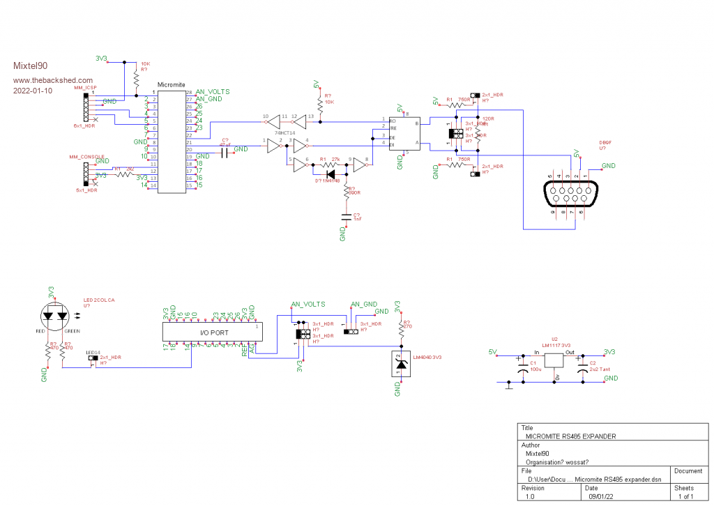 Edited 2022-01-10 04:59 by Mixtel90 Mick Zilog Inside! nascom.info for Nascom & Gemini Preliminary MMBasic docs & my PCB designs |
||||
| Tinine Guru Joined: 30/03/2016 Location: United KingdomPosts: 1646 |
Does anyone else find themselves staring at PCB images for unreasonable periods of time or is it just me? I could visit an art gallery of this stuff. I probably just need to get a life |
||||
| Mixtel90 Guru Joined: 05/10/2019 Location: United KingdomPosts: 7815 |
I've done a lot of it recently. LOL! I really should get out more... :) Mick Zilog Inside! nascom.info for Nascom & Gemini Preliminary MMBasic docs & my PCB designs |
||||
| Page 1 of 6 |
|||||
| The Back Shed's forum code is written, and hosted, in Australia. | © JAQ Software 2025 |
