
|
|
Forum Index : Microcontroller and PC projects : General purpose I2C IO module
| Author | Message | ||||
| Turbo46 Guru Joined: 24/12/2017 Location: AustraliaPosts: 1593 |
I do, how did you know?  Just checking, thanks. Bill Keep safe. Live long and prosper. |
||||
| Mixtel90 Guru Joined: 05/10/2019 Location: United KingdomPosts: 5735 |
Just a few points for those thinking of using HC-12 modules in the UK. As they come, out of the box, they are *illegal to use in the UK*. This is one of my pet peeves about them, being a radio amateur. You MUST reprogram them before use - and then you'll find that the range is *a lot* less than you may expect. You are not allowed to use a transmitting antenna with gain to get more range (but you can use one for reception only). They come set for +20dBm - 100mW output, but the UK maximum is 10mW. Use AT+P5 as a maximum to get 12mW, which is the closest you'll get. NZ/Australia allow 25mW. Channels 65,66 & 67 are in the UK radio control 459MHz band so avoid those. :) The official centre frequency for ISM in the UK is 433.92MHz and channels are in 400kHz steps. That means that only channels 1 (the default),2 and 3 are legal for the HC-12 in the UK. -------------------- I'm still progressing with all the boards in this series. Hopefully I'll be ordering some samples before too long. Mick Zilog Inside! nascom.info for Nascom & Gemini Preliminary MMBasic docs & my PCB designs |
||||
| Turbo46 Guru Joined: 24/12/2017 Location: AustraliaPosts: 1593 |
Hi Mick, I see that you are still being diverted But I am still keen to order some of your RS485 and Sea-of-holes boards when you are happy with them. I'm a bit more confident about ordering boards from JLB now and when they finally come I'd like to have another go.Bill Keep safe. Live long and prosper. |
||||
| Mixtel90 Guru Joined: 05/10/2019 Location: United KingdomPosts: 5735 |
erm... yeah... (Pleads insanity  ) ) I think I've gone over all the boards now, so they should all be ok. I've just given these a once-over just in case. :) Micromite 485 node 16_gerber.zip mini interface 12_gerber.zip Mick Zilog Inside! nascom.info for Nascom & Gemini Preliminary MMBasic docs & my PCB designs |
||||
| Turbo46 Guru Joined: 24/12/2017 Location: AustraliaPosts: 1593 |
Thanks for that Mick, I just have a couple of questions: If you have a look at the two connectors 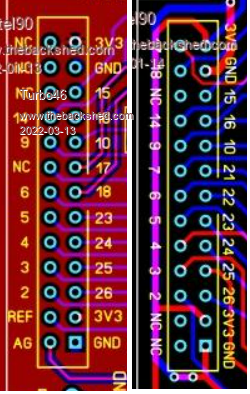 The one on the left is from the RS485 board and the other is from the sea-of-holes board. The pin numbers around the keyway are different. I have the feeling that the numbers on the sea-of-holes board are wrong and it has no real consequence as long as you use the numbers on the RS485 board which (I believe) are the MX170 pin numbers. Can you please tell me what the two holes are just under the connector on the sea-of-holes board? They look like vias side by side that do the same thing (for higher current rating?). It's hard to follow the tracks in places. I was hoping to use a connector like this: 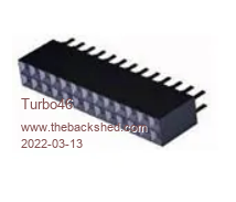 on the underside of the sea-of-holes board to mate with the connector on the RS485 board. Do you see a problem? Bill Keep safe. Live long and prosper. |
||||
| Mixtel90 Guru Joined: 05/10/2019 Location: United KingdomPosts: 5735 |
The number changes go deep. I've always tried to keep the maximum number of IO available but some are always used for comms and there aren't all that many available to start with. The "sea of holes" board is labelled as all pins being available. The 485 board needs COM1 RX, TX and EN (7, 21 & 22) for comms. The I2C board needs I2C_SCL and I2C_SDA (17 & 18) for comms. I2C is connected to the LH square of pins, 3V3, GND, SCL, SCA so that a 2x2 dupont connector can be used. (The RH square can take 2 vertical links: 3V3-REF and GND-AG if the internal option is set to External) When 21 and 22 aren't available I've moved 17 & 18 to their position and consequently sacrificed I2C connectivity. That allows pins with similar functions to still be available. In your case 7,21 & 22 are in use on the bottom board so you mustn't connect to them on the top one, but 17 & 18 are passed through (albeit in the "wrong" positions), so you could add a couple of pullups and link the boards over I2C. You should be able to stack the boards ok. You'll need 11mm spacers (it's a standard size), the holes are 3mm dia. Good guess at the vias. Bang on. :) They should be filled really, I suppose, but these are toys so I didn't bother with that. Mick Zilog Inside! nascom.info for Nascom & Gemini Preliminary MMBasic docs & my PCB designs |
||||
| Mixtel90 Guru Joined: 05/10/2019 Location: United KingdomPosts: 5735 |
I can't leave this stuff alone... I have two systems, the PicoMite VGA mini and the IO modules, that use the same 2x13 box header connector but with completely different pin arrangements. This incompatibility annoys me greatly, but I couldn't find a way of solving it - until now. :) The PicoMite VGA mini Version 3.0 has changed somewhat, but is in the same 90mmx70mmx28mm case: * The PicoMite is now across the case so that the USB lead can be plugged in without removing the PCB from the case. * The linear regulator has gone. * I've used Volhout's audio line output circuit - hopefully the noise level will be ok. * There are less IO pins used as there are less spare, but now any devices that would plug into the IO modules will now also plug in to this without going bang. Unused IO connector pins can optionally be connected to GND either directly or, preferably, using resistors. (Done as a mod - the holes are there). * The multiturn pot in the video circuit is now a sealed 6mm trimmer and a fixed resistor (easier to get). * The VGA socket is now the one used for the CMM2 (easier to get) * Links are fitted to disconnect the I2C pullups so those pins can still be used for I2C if the RTC isn't fitted. Alternatively they can be used for normal IO if the RTC isn't fitted and the links are disconnected. * The sea of holes and the expansion board have gone. * The audio jack has been moved to thr IO end. (I thought hard about this as it is blocked if an IO expansion module were to be plugged in directly, but GP6 and GP7 are on the IO port anyway so the audio can be in another box.) * Unlike the IO modules there is no 3V reference on the board, but REF and AGND are brought out so an external one can be fitted easily. That's it at the moment. :) EDIT: And now, if I've got it right, you can select the audio between line out and headphones using links on the board. No need to build one version or the other. Edited 2022-03-28 03:58 by Mixtel90 Mick Zilog Inside! nascom.info for Nascom & Gemini Preliminary MMBasic docs & my PCB designs |
||||
