Notice. New forum software under development. It's going to miss a few functions and look a bit ugly for a while, but I'm working on it full time now as the old forum was too unstable. Couple days, all good. If you notice any issues, please contact me.
Warpspeed Guru Joined: 09/08/2007 Location: AustraliaPosts: 4406
Posted: 11:12am 18 Mar 2017
Copy link to clipboard
Print this post
Klaus, What I have at the moment is one fully functioning 27 step inverter, plus one bare empty spare circuit board. My 2.9 Kw 81 step inverter is now complete with metalwork, transformers and wiring, but without any circuit boards for it.
I have the artwork file here ready to go, but just have not got around to getting any boards made. There is always something more urgent to spend money on around here.
I am about to pull the trigger on buying a 6Kwh Lithium battery which will wipe me out financially for a while, so no plans to get any of these boards made in the very near future.
If a few people are interested we could share the costs on some boards and do it that way.
Also, I can program anyone's 27C16's with 81 step data if they supply the eproms and return postage, and I will toss in a 3.2768 Mhz crystal for free as I have a hundred of them here I will never use.
If you combine a 3Kw transformer, a 1Kw transformer and a 330Va transformer you will potentially have a 4.33 Kw inverter. But it will output several times that for a short period, as transformer heating is not that rapid, provided there are enough mosfets in the primary to support the current.
Cheers, ĀTony.
Tinker Guru Joined: 07/11/2007 Location: AustraliaPosts: 1904
Posted: 10:55pm 18 Mar 2017
Copy link to clipboard
Print this post
Thanks Tony, that is very informative as usual. So I would have the cores for #1 & #2 transformers. #4 should be 110VA then, is that right?
With regard to the windings, I gather 230-240V for the secondary (output) and the battery voltage for the primary on all 4 transformers? Not some lower voltage primaries like on the ozinverters?
Is it OK to go a little over with the wire size, like aiming for a 5KW unit? Presently I'm running a modified PowerJack 8KW and that has not malfunctioned at all so far, regardless what I turn on in my workshop with the exception of the 175A MIG/TIG/Stick combie welder. This welder is not happy running from the inverter but runs fine off the mains. But I would like an equally rated inverter to have in reserve just in case something happens with the Powerjack clone.
Perhaps Grogster is interested to make some PCB's, he seems to be full bottle about them. I can only do single sided boards at home and your board appears to be too complex for that.
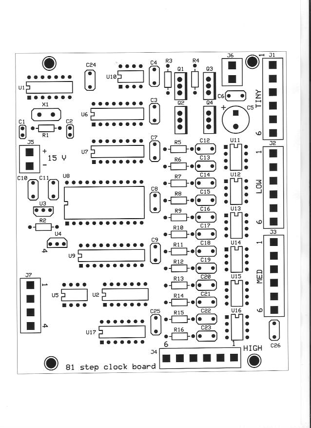
May I ask for a schematic what is connected to J1 to J4? I know its the mosfets but I like to study how you did that.
Thank you for your patience, this concept is very new to me and it looks like a nice project. Klaus
Madness Guru Joined: 08/10/2011 Location: AustraliaPosts: 2498
Posted: 12:57am 19 Mar 2017
Copy link to clipboard
Print this post
My method of toner transfer has worked well for me doing double sided PCB's, only thing I can't do is plate through. My solution to that is to leave via's pass wire through instead.
I print out the images on glossy paper with a laser printer and put the printed sides inwards, carefully line them up with a bright light behind and staple them together. Cut the PCB to size without touching it with your bare hands at any stage prior to heating, scratch up the surface with 180 grit sandpaper and then clean with acetone. Once dry (wet acetone will dissolve the toner) put the PCB between the sheets of paper and run through a preheated laminator at full temperature several times. Then I put the PCB in the oven at 180 for 5 minutes while the laminator is on. Take it out of the oven and straight through the laminator a couple more times. I know of at least one person who has done this with an iron rather than the laminator. The baking in the oven is important to get a nonporous layer of toner.
Dunk it straight into cool water and let it soak for a while. Then rub off the paper, if you have done everything properly the toner will be very robust and will not rub off under your fingers. Once the paper is off let it dry, if there has been any imperfections touch it up with fingernail polish. Then etch it, I use 2 parts peroxide to one part hydrochloric acid, this will etch it quite quickly when first used. It will regenerate with oxygen from the air over time and you can use it many times, however it does get much slower.
Once etched clean off the toner with acetone and drill the holes. I have found this method lines up quite well worst I have had is within about 0.25mm, most times it aligns so close you can't see any difference in alignment. I can print a new design, transfer toner etc to double sided 2oz PCB and be drilling it within 45 minutes.
PS
I use Designspark to do the PCB design, it was a bit of a learning curve but works great now I have got the hang of it. It is free and there is no size limit, so I can do a 200 X 300MM inverter PCB with no problem.Edited by Madness 2017-03-20There are only 10 types of people in the world: those who understand binary, and those who don't.
Tinker Guru Joined: 07/11/2007 Location: AustraliaPosts: 1904
Posted: 02:53am 19 Mar 2017
Copy link to clipboard
Print this post
Thanks mad for the PCB making tips. I actually tried making a double sided PCB by the toner transfer method last week. I did the alignment different though. One side at a time was laminated on, the second side aligned to tiny corner holes I carefully drilled into the first side.
It was OK but nowhere near as accurate as you claim. However, I got thoroughly confused with the mirror images the toner transfer method produces. So in the end the location of the gate & source pins were accidentally swapped on the artwork and the board unusable.
I do, however, not bother with an oven. I think your method of getting the toner to stick to the PCB is doing it the hard way.
So, as you mentioned, using an iron is a waste of time - it simply does not work.
Using a laminator is the way to go but *do* modify the laminator first so it runs hotter. That was discussed here a few years ago. The only really suitable laminator was the Lowell brand, it has spring loaded rollers and can cope with a 1/16" thick PCB board.
Using that with two runs through it is sufficient. But, the toner is actually quite porous. So I use a product called TRF (toner resist film) as a secondary treatment. This puts a green layer over the black toner that hides the porosity very well. Any imperfections due to scratching or dust are now easily spotted and corrected with a PCB marker pen.
I used to use ferric cloride but its now exhausted, its also very messy. I bought that ammonia something granules to try next time. They need to be dissolved in rather hot water, my etching tank has a heater fortunately. If that does not work well I'll try your etching recipe. Klaus
Warpspeed Guru Joined: 09/08/2007 Location: AustraliaPosts: 4406
Posted: 10:26am 19 Mar 2017
Copy link to clipboard
Print this post
The logic behind the transformer design will go something like this.
For 5Kw we are looking at creating 240v rms at say 21 amps rms. That will require a peak output voltage of 340 volts. To generate 340 volts, the combined voltages of all our secondaries must add up to 340 volts when all the inverters switch on together in the same direction.
Our inverters need to have output voltages where each successive inverter has exactly one third the output voltage of its predecessor.
So for four inverters the voltage of the largest will be X volts. The next stage down requires 1/3 X or 0.333X secondary voltage. Third inverter will be 1/9 X or 0.111X secondary voltage. Fourth inverter will be 1/27 x or 0.037X secondary voltage.
If all four inverters switch on simultaneously the output voltages all add together. 1.0X + 0.333X + 0.111X + .037X = 1.481X Now we know 1.481X must equal 340 volts So X needs to be 340/1.481 = 229.6 volts.
(If there were only three inverters 1.444X would equal 340 volts. And X would be 235.4 volts).
For four inverters the largest transformer will need a square wave secondary voltage of 230 volts and a rated current of 21 amps for 5Kw.
The next stage down will be 1/3 of that or 76.666 volts, also at 21 amps rms.
Third stage 1/9 of 230 volts or 25.56 volts at 21 amps rms.
Fourth stage 1/27 of 230 volts 8.52 volts at 21 amps.
We are dealing with only square wave voltages, so rms voltage is not applicable. We just use square wave peak voltages for calculating the transformer ratios.
But the secondary current will be a sine wave !! And that current will always be there in each secondary, even when a particular inverter is outputting zero volts (shorted clamped output) so we must use the 21 amp rms secondary current for calculating secondary wire sizes.
The largest transformer with 230 volt secondary is most fortunate, because we can use an existing transformer primary as our secondary. And with luck we might be able to use the second original winding as the clamping winding. That then only requires the addition of a new low voltage primary to suit our battery voltage.
The problem might be that there is simply not enough room left for a heavy enough third primary winding. In that case we may be stuck with having to use just the original 230v winding already there, and our new big welding wire primary, and put our fully floating zero volt clamp right across the 230v secondary where the current will only be 21 amps rms maximum.
All this should be pretty familiar territory, and if you already have a failed PWM project, the chances are that the transformer you already have will work with just some additional primary turns added to it.
The PWM transformer needed to generate 340 volts peak from the original battery, we only need to reach 230 volts peak from the same battery voltage, so about 40% more primary turns will be required than on an Oz inverter transformer. This is very good, because it reduces the flux swing in the core by 40%, and that will be hugely beneficial to reducing inverter no load idling current.
All this is the very first thing to do. Get just the big inverter going by itself, and test it with a 20 amp load so you get a 230v peak square wave output, and make sure all is well. I would expect the idling current to be very low, and that will be a very interesting thing to see.
I will go into details of the other transformers later. The big one is going to be the most difficult only because of its size and weight.Edited by Warpspeed 2017-03-20Cheers, ĀTony.
Madness Guru Joined: 08/10/2011 Location: AustraliaPosts: 2498
Posted: 11:11am 19 Mar 2017
Copy link to clipboard
Print this post
Klaus I have tried aligning to holes and putting on the second side however the paper does stretch slightly as it goes through the laminator. It is not an issue for individual components but over the length of a PCB it gets worse. I have found that toner transfer stuff expensive and the oven works fine for me and is not difficult.
I modified the first laminator I had to get it hotter but the rubber rollers bubbled up. Fortunately I found another at the tip shop that heats to 230 standard, it is a commercial quality Fordigraph machine. It runs a litle fast and I need to work out how to slow it down one day.
As for mirroring, print the bottom layer as you see it on your screen and mirror the top the layer.
I have made quite a few PCB's this way now and have not had one failure using this method.There are only 10 types of people in the world: those who understand binary, and those who don't.
Warpspeed Guru Joined: 09/08/2007 Location: AustraliaPosts: 4406
Posted: 11:20am 19 Mar 2017
Copy link to clipboard
Print this post
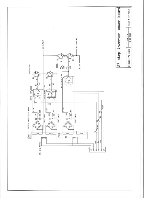
Oh sorry Tinker I almost forgot. J1 to J4 are the outputs to each of the four inverters.
Pins 1 and 2 provide +/- 15v at 50 Khz continuous square wave power to provide isolated dc voltages for the mosfet gate drivers via small pulse transformers. I did it that way because I already have a quantity of suitable pulse transformers I wished to use up. There are different and much better ways to do it, but it suited me to do it that way at the time.
Pins 3 and 5 are drive to the inverter which could be half bridge, full bridge, or push pull topology.
Pin 4 drives the zero volt clamp, it provides the third "off" state for the inverter when it is not being driven "on" in either direction.
The whole thing has been an evolving project, and originally I planned to use push pull inverters with a floating clamp winding. That meant all my mosfets would have had grounded sources, and this clock board could drive the mosfet gates directly.
A much safer way, especially for higher voltage or higher power, is to use the outputs of the ICL7667 mosfet gate driver chips to drive opto isolators, they are perfect for that. and that is how I recommend all the mosfets be driven.
If every mosfet gate has its own fully isolated gate driver, it solves a lot of grounding and noise problems. It also minimises fault escalation if something blows up.
Nothing worse than having +48 volts find its way back to the +5v rail through a chain of exploded chips. If the power stage is isolated by optos or pulse transformers, any destruction stays pretty well localised.
I tried to post the schematic of my power board, but the server comes up with an error. Will try again later.Edited by Warpspeed 2017-03-20Cheers, ĀTony.
mackoffgrid Guru Joined: 13/03/2017 Location: AustraliaPosts: 460
Posted: 12:41pm 19 Mar 2017
Copy link to clipboard
Print this post
Thanks Tony
Looking forward to trying this out.
It's pretty handy if we can re-use the 240V winding on the aerosharp transformer. I can't remember if the low voltage winding was on the outside - allowing us to strip that winding off and leaving the 240v winding.
Working on my schematic yesterday, I did add capability of regulation (I realized a mistake in a previous post - 27c512 gives 32 steps of regulation) because I can. Also adding an arduino nano so I can do pretty things like a display, remote comms, extra sensing. However - the inverter will be able to work without the nano.
I'm working on using the TLP250 opto Fet drivers (which will be on the FET board). I presuming you are using the 7667's as line drivers and not switching any FETs with them?
mackoffgrid Guru Joined: 13/03/2017 Location: AustraliaPosts: 460
Posted: 01:16pm 19 Mar 2017
Copy link to clipboard
Print this post
Tony, you answered my questioned regarding the 7667s before I asked it
Warpspeed Guru Joined: 09/08/2007 Location: AustraliaPosts: 4406
Posted: 02:24pm 19 Mar 2017
Copy link to clipboard
Print this post
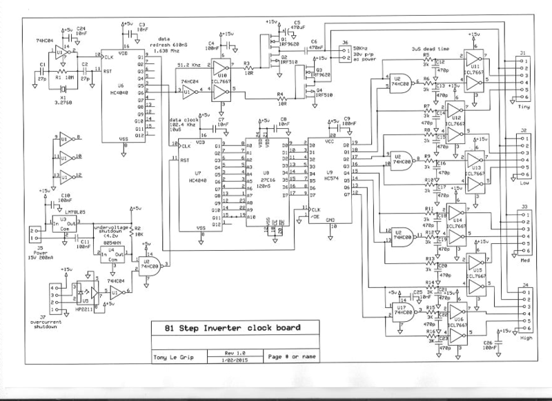
Those 7667's are really good to use, the input logic threshold is 1.5v not 2.5v as is usual for most 5v cmos logic chips. That enables us to use a simple RC integrator to generate dead time without needing a diode. The output switches very fast rail to rail and has a ton of drive capability. They do however invert the signal, so data in the eprom has to be the compliment (inverted) to what we eventually require.
Output at the J1 to J4 connectors is the more useful logic hi = mosfet on.
Cheers, ĀTony.
mackoffgrid Guru Joined: 13/03/2017 Location: AustraliaPosts: 460
Posted: 02:54pm 19 Mar 2017
Copy link to clipboard
Print this post
That is cool, I've used them in my solar regulator. I did wonder why you didn't have diodes there.
Did you do any cross conduction protection on the FET board?
Warpspeed Guru Joined: 09/08/2007 Location: AustraliaPosts: 4406
Posted: 04:33pm 19 Mar 2017
Copy link to clipboard
Print this post
Those 7667 chips also have a Schmidt trigger input for jitter free dead time.
Cross conduction is only likely to be a problem during power up and power down, when the various power rails are slowly changing in an unpredictable manner. Undervoltage chip U4 holds the main counter in reset at 4.2 volts and under. Do not leave this feature out !!!
If doing all this inside a microcontroller, power up and initialisation of the port should be pretty straightforward. But powering down may have some hidden problems. Careful thought needs to be given to what happens if you reset the microcontroller with the software running. It should be o/k but it is something to think about.
I found a sneaky way to add cross conduction protection to the opto isolators on the FET board. Will try again to post the circuit. I think the Forum server needs its nappy changed.
Edited by Warpspeed 2017-03-21Cheers, ĀTony.
mackoffgrid Guru Joined: 13/03/2017 Location: AustraliaPosts: 460
Posted: 06:16pm 19 Mar 2017
Copy link to clipboard
Print this post
Definitely have put the supervisor in.
I'm not doing that function in the nano but it can. I have connected a pin from the nano into that circuit so I can execute over current or other errors from the nano.
I want the circuit to work without the nano should I desire.
I like sneaky ideas look forward to seeing it.
Tinker Guru Joined: 07/11/2007 Location: AustraliaPosts: 1904
Posted: 01:26am 20 Mar 2017
Copy link to clipboard
Print this post
Hi Tony, I'm slowly getting my head around this , thanks for your excellent explanations. So the secondaries (output) windings are in series. Makes sense when I think about that for a bit. The full load current runs through all windings, meaning a hefty wire size.
Now I'm stuck with the "clamping winding" you mentioned. Any chance of a sketch of a typical transformer's windings and their voltages, say for the biggest transformer?
I'll have to go back on your messages now to see if you explained the clamping function with respect to its associated winding. You did mention that you used stock transformers from Altronics, did you add windings to these?Klaus
Warpspeed Guru Joined: 09/08/2007 Location: AustraliaPosts: 4406
Posted: 07:38am 20 Mar 2017
Copy link to clipboard
Print this post
Tinker,
We are connecting four different "power sources" in series to drive a load. By switching them on and off in a particular sequence we can make them add or subtract to generate voltage steps.
But we cannot just open circuit the individual supplies we do not need when they are connected in series. The unused supplies must be SHORTED OUT to provide a continuous current path through the series string.
The basic building block to do this, is a bi directional ac on/off switch using either mosfets or IGBT's. Both the sources and the gates are tied together.
When both mosfets are off, the switch is open circuit in either direction . When both mosfets turn on together, we get current flow in either direction with one diode voltage drop.
For higher voltages IGBTs are preferred over mosfets, but the particular IGBTs must have the inverse diodes fitted. Some have these internally, some do not. Mosfets all have internal inverse diodes.
Still cannot upload pictures.................
[quote] HTTP Error 500
Oops! Looks like the page you wanted has a error...
The server has an issue, or two. An email has been sent to the site owner, he'll go grab his hammer and fix it up real good. Please click your browsers BACK button, or go to the home page.
http://www.thebackshed.com [/quote]
Cheers, ĀTony.
Warpspeed Guru Joined: 09/08/2007 Location: AustraliaPosts: 4406
Posted: 07:59am 20 Mar 2017
Copy link to clipboard
Print this post
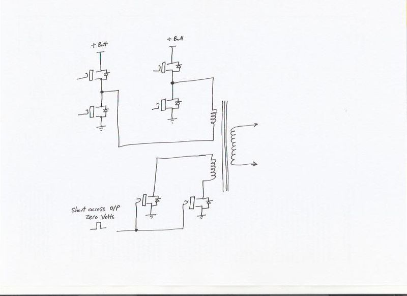
O/k I will try doing this through Photobucket. Hooray it works. Now one of the three (four) power boards. Notice that the opto isolators are connected in inverse parallel between the +ve and -ve drivers. It is impossible for both to turn on together. The NAND gate U2 on the clock board pretty much guarantees that the clamp cannot operate if either +ve or -ve driver is active. Its the last line of defence for a spurious cross conduction accident if the eprom data corrupts.
Here is the 81 step schematic again, it might come out a bit higher resolution.
Edited by Warpspeed 2017-03-21Cheers, ĀTony.
mackoffgrid Guru Joined: 13/03/2017 Location: AustraliaPosts: 460
Posted: 10:02am 20 Mar 2017
Copy link to clipboard
Print this post
Thanks Tony Cross conduction prevention is simple and clever, I like it.
Tinker Guru Joined: 07/11/2007 Location: AustraliaPosts: 1904
Posted: 11:03pm 20 Mar 2017
Copy link to clipboard
Print this post
Thanks Tony,
I see why the PWM inverters are more popular nowadays, way less complicated IMO .
So, from dim memory, a short on the primary winding translates into a short on the secondary with transformers? So, is that extra primary identical to the other which drives the transformer? Klaus
Warpspeed Guru Joined: 09/08/2007 Location: AustraliaPosts: 4406
Posted: 11:25am 21 Mar 2017
Copy link to clipboard
Print this post
The third winding can be made any voltage you like, its either open or shorted, and the open circuit voltage does not matter.
But current in the shorted winding and through the mosfets or IGBTs doing the shorting needs some consideration.
Its a lot easier to short out 10 amps at 500v than 500 amps at 10v. At ten amps only a single pair of pretty ordinary IGBTs would do that easily and efficiently, with minimal heat sinking and fewer devices.
Five hundred amps would need some pretty serious mosfet hardware to achieve the exact same final result.
All my clamps are right across my high voltage primaries, where there is very little current to clamp. So its very efficient and very easy to do.
You guys will be doing it all a bit differently because there is going to be a low voltage primary.
I think the easiest to do and the most practical solution with a big toroid would be to just add a welding wire primary to the existing 230v secondary that is already there. That will allow maximum room for a really decent primary.
Then clamp right across the 230 volt secondary with a single pair of IGBTs that have internal diodes. That will require an opto isolator gate driver, and an isolated 15 volt dc supply, so that the clamp is entirely floating. Pretty much the same as I did. We are not switching at 20 Khz, so a small wimpy 1A gate driver is all we require for driving our clamp IGBTs.
The advantages are that the current through the secondary be low (20A for 5Kw maximum)and it is pretty easy to do.
The clamps on the smaller transformers can be done differently if we choose. We can look at all that once we have the big inverter up and running.
Once you are ready to test your big toroid, first put on a primary using very thin wire to find out how many primary turns will be needed to reach 230v across the secondary. Once you know the number of turns (and roughly the required wire length) it a lot easier to decide what may actually fit into the available space. This will require more primary turns than an Oz inverter application, so expect a greater length of thinner wire will be required on the primary in order to fit.
And its better to know what to expect before you start winding, as its a pretty physically demanding job. Cheers, ĀTony.
mackoffgrid Guru Joined: 13/03/2017 Location: AustraliaPosts: 460
Posted: 11:55pm 22 Mar 2017
Copy link to clipboard
Print this post
Hi Tony
I'm am pretty much on the same page re: clamping.
I spent the day preparing the main transformer.
In case it helps others I am logging here the features of the transformer.
It was out of a 3kW aerosharp, weighed approx 17kg out of the box. Its windings are primary 230v to secondary 250V. The secondary is one the outside layers. The secondary consists of 3 parallel windings of 1.4mm dia. (over enamel, assuming 1.3mm dia copper /i calculate 1.33mm2 each or 4mm2 total )
I removed all of the secondary windings except for 30 turns of one wire for testing purposes. I'm assumming its wound for approx 1 volt per turn. Will find out soon enough. (i'm shooting for 27v : 235v)
All going well the existing primary will work well. I can't tell but i presume it is at least the same sqmm of conductor as the secondary.


 , thanks for your excellent explanations.