
|
|
Forum Index : Electronics : Various aspects of home brew inverters
| Author | Message | ||||
| poida Guru Joined: 02/02/2017 Location: AustraliaPosts: 1432 |
I am running continuous current through the devices to create some heat. I know the inverter pulses 100% ON then 100% OFF. I know I am running them in the saturation zone where they are maybe 30% ON. I am unconcerned with this difference. I want to generate some heat and see how well this heat is conducted away from the internal silicon. I agree that at times a full bridge inverter will see very large currents. If there is an adequate primary winding inductor, then the current seen will be of the order of the output power / primary voltage. 6kW output at 50V supply from the battery implies to me approx 120 Amps average primary current. If the duty cycle of the SPWM is maybe 70% then we divide this 120 A by 0.70 to get pulse current, maybe 170A. If the primary winding inductor is not good enough( i.e. it saturates at 170A or lower), it will no longer be 170A, it would have peaks of short duration but much higher currents, maybe 2-5x this average. And this is running at a steady 6kW. Then Oztules pulls the trigger on his MIG welder and the current goes through the roof. wronger than a phone book full of wrong phone numbers |
||||
| poida Guru Joined: 02/02/2017 Location: AustraliaPosts: 1432 |
I drive the gate from an op-amp. The op-amp is taking a set point voltage, maybe 0.5V and amplifiying the difference of that with the voltage across a current sense resistor. The op-amp output is then fed to the mosfet gate. This way you can control the current flowing through the current sense resistor and the mosfet simply from a pot. typical gate voltages for 2 Amp with my current sense resistor and op-amp gain are 4.2V when I am testing/breaking a HY4008 TO-220 fet. I hooked up the DSO, to show current sense voltage and gate drive voltage. Let's break another fet... supply voltage is 30V, i.e. Drain - Source voltage. Yellow is gate voltage. 2V/div Pink is current sense voltage across a 0.22R resistor. (0.22V = 1 amp) The timebase is 0.5 seconds/div 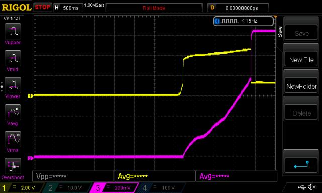 You can see I drive the current from zero to about 4 amps over 3 seconds as I turn the pot. Then the current rapidly rises to about 6 amps, the power supply max set point. I broke the mosfet. This device is specified to handle DC currents of 200A at 20Cj (junction) and 144A at 100Cj. There is a graph showing safe operating area, which combines max volts, max amps and safe operating area. 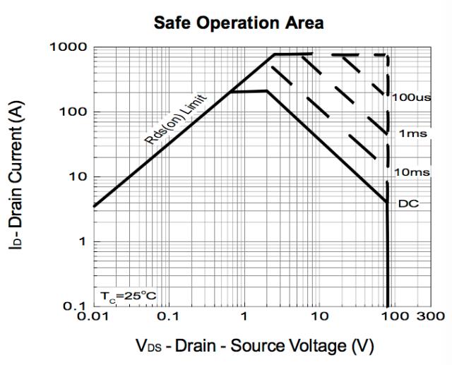 At 30V the SOA shows I can put about 9 amps through the device. And yet I killed it putting 3.6A through it. (0.8V / 0.22 R) wronger than a phone book full of wrong phone numbers |
||||
Madness Guru Joined: 08/10/2011 Location: AustraliaPosts: 2498 |
Need to be careful what I joke about.  There are only 10 types of people in the world: those who understand binary, and those who don't. |
||||
| Madness Guru Joined: 08/10/2011 Location: AustraliaPosts: 2498 |
So Poida you have established HY4008s are crap as heaters. Have you thought of turning them on fully and seeing how much current you can get through them before they fail? Has anyone killed them by overloading them? Talking with my educated uncle the other day he said the weak link is the gold or tin internal connectors, I am sure we would be lucky to have tin at the price of these. There are only 10 types of people in the world: those who understand binary, and those who don't. |
||||
| Tinker Guru Joined: 07/11/2007 Location: AustraliaPosts: 1904 |
Just out of curiosity I googled the mosfet (NEC K3304) poida was testing and found the excellent the heat transfer properties of. Well, its like comparing apples to oranges. That mosfet is a high voltage, low current and rds on 2 Ohm device. What would be of much more interest to me is a comparison of an alternative to the HY4008 mosfet that has similar parameters. Does anybody know of one in a TO247 package? I can't positively say I managed to kill the 4 HY4008 mosfets of an early experimental set up by current overload or some other cause when I tried to push them beyond 2KW... But I now see the importance of a heatsink better being oversize than relying too much on fan cooling. A thick heatsink back to suck up the spot heat before it gets to the fins where the fan does its cooling thing. Klaus |
||||
renewableMark Guru Joined: 09/12/2017 Location: AustraliaPosts: 1678 |
I'm not too keen on thinking about that sort of thing, but hey you go for it. Cheers Caveman Mark Off grid eastern Melb |
||||
| poida Guru Joined: 02/02/2017 Location: AustraliaPosts: 1432 |
I am looking at IRFP4110 and IRFP2907 and just ordered a pair of each. I will run both of these up to 2/3 of max current at 30V inside SOA to see how the heat will be conducted away from the chip. On review of the specifications - maybe I shouldn't. 4110:  2907:  Heat sink choice for me would require a balance of MOSFET mount point thickness and fin area. Small fin area means a better fan and running it more often. wronger than a phone book full of wrong phone numbers |
||||
| Madness Guru Joined: 08/10/2011 Location: AustraliaPosts: 2498 |
Klaus here is some that are similar Budgetary Price €�/1k 1.56 ID (@25�C) max 180.0 A Mounting THT Ptot max 370.0 W Package TO-247 Polarity N QG (typ @10V) 150.0 nC Qgd 43.0 nC RDS (on) (@10V) max 4.5 mΩ RDS (on) max 4.5 mΩ RthJC max 0.4 K/W Tj max 175.0 �C VDS max 100.0 V VGS(th) min max 2.0 V 4.0 V VGS max 20.0 V and this one runs rings around the HY4008W. Budgetary Price €�/1k 3.35 ID (@25�C) max 350.0 A Mounting THT Ptot max 520.0 W Package TO-247 Polarity N QG (typ @10V) 380.0 nC Qgd 105.0 nC RDS (on) (@10V) max 1.8 mΩ RDS (on) max 1.8 mΩ RthJC max 0.29 K/W Tj max 175.0 �C VDS max 75.0 V VGS(th) min max 2.0 V 4.0 V VGS max 20.0 V Both cost 3 times as much. There are only 10 types of people in the world: those who understand binary, and those who don't. |
||||
| Warpspeed Guru Joined: 09/08/2007 Location: AustraliaPosts: 4406 |
All this raises quite a few issues, but heat flow is really where the rubber meets the road as far as how far you can push the part. A few random thoughts... Just because it has the big TO247 package does not mean it is any different internally to what you get inside a smaller TO220 package. How the manufacturer has bonded the silicon to the copper back plate is important, but also so is the basic area of the silicon die in contact with the backing plate. How many silicon dies you can fit on a full wafer is a very big part of the manufacturing cost. So shrinking things down a bit means more profit. The Chinese can make up some mosfets and stamp any part number they like onto the outside. If it roughly complies with some industry standard part, that is probably good enough to sell AS that part. It may even come very close for RDSon and voltage rating, but it may fall a long way short on other important parameters that may be critical for a particular intended use. Quality control comes into it too. Dragon brand mosfets might be rather different inside from one manufacturer to the next, or one batch to another. They are cheap, but even then you may not be getting what you pay for. Safe operating area is what we should be looking at. This is especially important for bipolar transistors, but mosfets have their limits too. Fortunately with mosfets the RDSon increases with temperature locally, so the current tends to even out across the silicon die. It then becomes a much more simple thermal conductivity and heat flow problem. If Mr Foo has cleverly made his silicon much smaller and bonded it to the copper backing plate using inferior materials and methods, we might be in trouble trusting the safe operating area curves very carefully produced by a genuine Western manufacturer. I really do not know the answer to this, as genuine parts are so much more expensive than the fake stuff. I suppose its bad practice anyway to run parts right up to their absolute published limit and expect them to work reliably for any length of time. All we can do is use the published data and curves, properly engineer the application with a generous safety margin, and hope.... Cheers, �Tony. |
||||
| Madness Guru Joined: 08/10/2011 Location: AustraliaPosts: 2498 |
Using an infrared thermometer I have found the front of the HY4008Ws to be less than 5 degrees warmer than the heatsink while my inverter is working hard. There are only 10 types of people in the world: those who understand binary, and those who don't. |
||||
| wiseguy Guru Joined: 21/06/2018 Location: AustraliaPosts: 1206 |
Poida I am not sure that your method of testing is totally valid with regards to the SOA & internal heat being generated. My understanding of FETs designed for high speed power switching is that they are quite unsuitable for operating power throughput anywhere near their linear region. I believe that switching FETs can usually be thought of as a mass of multiple cells all in parallel. The characteristics of each cell is very similar but there lies the problem. If the gates are all driven hard into their on region the on resistances are all combined into an extremely low value - so far so good. However at the onset of their linear region (such as a controlled current sink) their may be just a few cells that begin conducting before the others begin to conduct & they can "hog" the current locally. Another mechanism that then makes this situation worse is that the gate threshold voltage has a negative temperature co-efficient, so any hot spots internally become much worse as their on voltage is now lower than previously so they ensure they will continue to hog more and more current until something gives. This failure mode is not really indicative of a FETs actual switching behaviour ability or its ability to transfer generated heat to the heatsink. Also internal hotspots are not the same as having an equivalent distributed-power heat spread evenly across the whole die I am not a FET expert but I think it is the VFET structure that lends itself to better linear current handling and are normally used in FET (linear) amplifiers. I think that a better method to test the heat transfer from across the whole die is to fully enhance the turn on of the FET using say a constant +12V and generate the heat from a shipload of current delivered from a single turn winding of a big toroid and a Variac. Half wave rectification no filter caps etc for the purposes of this application would be fine I think. 10W can easily be generated from say 50A with a 4 milliohm mosfet - the DC voltage to do this though will be ~ 200mV. 100A in the same setup will cause 40W. The test rig can then be easily used to test various other mosfets behaviour. I am not criticising your work just trying to ensure that testing is valid, repeatable and meaningful. If you already knew this stuff ignore my post. I also cant relate completely to their SOA & graph there are some discrepancies - including your ability to kill them with 5A! Maybe they are supposed to include switching data & timing into their SOA graph which appears to promise much better DC performance than you found - I dont follow why they suggest a hefty DC SOA and other information suggests to avoid this condidion ? Anyone interested in reading up on this stuff - 2 app notes AND8199-D & APT0403 If at first you dont succeed, I suggest you avoid sky diving.... Cheers Mike |
||||
Revlac Guru Joined: 31/12/2016 Location: AustraliaPosts: 1153 |
Ok When I looked at fets for various purposes I usually see the description and what it is used for, quite often I see they call them a high speed switch, and I would think that would be the best use for that particular fet and not so good in their linear region. So we want a switching fet, best suited for inverters. I do like these HY4008  and the VFET structure would be better suited for a power reg or powering fans or other thing's if not using PWM. these HY4008 when fully enhance the turn on of the FET I have seen them handle quite a few AMPS. Not sure of there limit tho Cheers Aaron Off The Grid |
||||
| Tinker Guru Joined: 07/11/2007 Location: AustraliaPosts: 1904 |
Assuming you have sanded off the black anodising from your heat sink, to make a good electrical contact to the mosfet back plate, your infrared thermometer might mislead you. These things are colour sensitive AFAIK. Can you try that test again but now blacking out the area around the test mosfet with a texta pen? Now the measurement should be between the black mosfet body and the blackened heatsink section. I would be curious if and what the difference is to your previous test. Since we already use a very good heatsink (if its out of the 3KW Aerosharps) which has a 10mm thick base plate any further heat transfer improvement (ignoring fans for the argument) would be the location of the mosfet mounting screw, Ideally it wound be in the center line of the base plate so any localised heat gets sucked evenly to the fins in all directions. If the screw is too close to the base edge, the mounting spot would become less ideal. Which tells me having longer mosfet legs is not such a bad idea as one builder here seems to think. Anyway, its all a compromise one way or another. Klaus |
||||
| Madness Guru Joined: 08/10/2011 Location: AustraliaPosts: 2498 |
Tinker that was on a Aero-Sharp heatsink that was sanded where the MOSFETs make contact, the rest was black still. I cut the heat sinks so they only have minimum clearance with the PCB with the MOSFETs inserted as far as they will go into the PCB, the way they are designed to be used. I wonder how hot those long legs are that you have a fetish for. There are only 10 types of people in the world: those who understand binary, and those who don't. |
||||
| Tinker Guru Joined: 07/11/2007 Location: AustraliaPosts: 1904 |
And I wonder about that inserting as far as it will go thing of yours .If the mosfets were, as you say, designed to be inserted "as far as they will go" into the PCB then why do the makers put long legs onto them? Me thinks you are on shaky territory with that theory. I did not know about your selective heatsink sanding, fair enough, this had never occurred to me. Much easier to sand the whole heat sink before its cut with a random orbital sander to 180 grit. Klaus |
||||
| poida Guru Joined: 02/02/2017 Location: AustraliaPosts: 1432 |
I agree that what I am going is nearly pointless. The MOSFETs operate fully ON and OFF for nearly all the time they are in service. But I wanted to see how well heat is removed from the packages. So I need to make some heat. I doubt there is any difference in the locations (within the MOSFET structure) where heat is generated as Vgs varies. So I chose to make a bit of heat with low Vgs since the current levels would be much, much lower - easily produced on the bench. I was concerned about longevity of the HY4008 and we know that heat is one enemy. At 25Cj (junction) the HY4008 can switch 200A but this rapidly reduces to 153A at 100Cj then down to 40A at 160Cj. I thought it prudent to see how well heat is carried away from the junction. If it was not so good at this task then we might be running these chips at junction temperatures MOSFET chip designers would term "exciting". I can repeat ad nausem the demonstration of a too hot to touch HY4008 (TO-247 package) when it is running at about 4.2V Vgs and 2.5A at 30V, about 75W. I sanded with a flat, hard mandrill + 1200 grit wet&dry the two mating surfaces: the heatsink and the back of the TO-247 package. I apply some heat paste and screw it down. After 30 seconds, I feel slight warmth from the heat sink and too hot to touch front of the MOSFET. After some time, things equilibrate to some extent. My fears are of a large current pulse drawn from the inverter, causing a large DC current pulse to be switched. This might occur over 0.5 to 1 second as a fridge motor starts. This sudden increase in heat is added to the existing temperature of the junction. Which I doubt is the same temp as the heatsink. What sort of thermal impulse headroom do we have here? The specs give thermal resistance of 0.38C/W junction to case. I am afraid I have to say I doubt this value. I also understand the modern switching power MOSFET is made up of many cells on the die. And that some cells will conduct more than others during Vgs voltages in the transition zone from OFF to ON. Certainly something I need to consider. I have previously thought of a fully ON test as you describe. I could hold the gate at 12V and run the house inverter supply through it, put a kettle on... 50A through 3mOhm is 7.5W (edit:whoops, not 0.15W) I would need more current, yes? this shows the V-I curve. Even at 260 Amps it's 1 V or 1/250 or 0.004 Ohms At 50Amps the curve looks steeper, i.e. lower resistance. 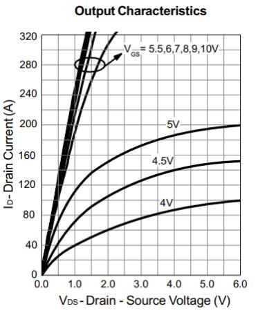 My battery is 8 x 200Ah Narada 12V, 2 series strings of 4. The inverter is good to 3000W maybe, on a good day with a fair wind. How to draw a controllable 200A.... But seriously, the TO-247 package can only handle about 75A due to the leads. I value highly your thoughts Wiseguy. wronger than a phone book full of wrong phone numbers |
||||
yahoo2 Guru Joined: 05/04/2011 Location: AustraliaPosts: 1166 |
I spent a couple of years thinking about this and got basically nowhere. I proved that I could progressively damage a mosfet several different ways and it would fail later at a seemingly low power/heat. the manufacturers supplied their estimation of the temperature where junction damage occurred and the speed of heat dissipation into the material around the junction. I could not work out the temperature differential and dissipation from that zone across to the heatsink. Seems to be some lag/feedback loop effect that retains heat close to the die. then the price of mosfets dropped 10X and I figured I was wasting my time. I'm confused, no wait... maybe I'm not... |
||||
| wiseguy Guru Joined: 21/06/2018 Location: AustraliaPosts: 1206 |
Poida, I value your thoughts efforts and input to the forum also. If at first you dont succeed, I suggest you avoid sky diving.... Cheers Mike |
||||
| Warpspeed Guru Joined: 09/08/2007 Location: AustraliaPosts: 4406 |
We really have two problems here. First, we cannot really define the operating conditions of an inverter, because we have no idea what can be plugged into it, or what kinds of fault or transient maximum loads are going to be experienced. Something out there will probably be "bad" enough to break your inverter at some stage. Second, because we have multiple manufacturers and suppliers of mosfets, we can never be absolutely certain that the mosfets we purchased cheap and in bulk even come close to the specified ratings and characteristics published by a completely different (and reputable) manufacturer. We really have nothing definite on which to base a proper systematic design. Cheers, �Tony. |
||||
| Madness Guru Joined: 08/10/2011 Location: AustraliaPosts: 2498 |
All HY4008Ws I have used have come from this supplier. I know many others have ordered from them as well, I have never had one that is bad out of the box and AFAIK no one else has. Can't be 100% sure that they all come from the same source but the consistently good results would indicate something is consistent. Any failures I have had have been from issues external to the Inverter. I know Oztules uses the same supplier and can start a 5KW single phase induction motor without any dramas. I have tried to start a stalled (I did not know it was stalled) 5KW AC compressor and it just popped the 20A breaker in the switchboard for the circuit, the house was running of the Inverter at the same time. If there was any hiccup I would have heard about it as I know my son was playing Xbox at the time. What has caused failures for me is a GTI failure that sent 400+VDC across the Inverter secondary. Someone else I know who I built an inverter for killed it as a result of running it via a resistance (don't ask). Oztules mentioned at least one failure due to very low battery voltage as well. What I am getting at is the MOSFETs are tough enough to trip a 20A AC breaker without blinking an eye. The only failure I have had directly from an overload was from a faulty oven we had, it had tripped a breaker and I reset the breaker and the inverter failed. This I think could be that for some reason that breaker won't trip until fully turned on. On that circuit is the entire except for AC & HWS, so there were 2 fridge compressors and a water pump to start as well. I have since adjusted the over-current shutdown to prevent this. Since then I have not had any failures. There are only 10 types of people in the world: those who understand binary, and those who don't. |
||||
| The Back Shed's forum code is written, and hosted, in Australia. | © JAQ Software 2025 |
