
|
|
Forum Index : Electronics : Various aspects of home brew inverters
| Author | Message | ||||
mackoffgrid Guru Joined: 13/03/2017 Location: AustraliaPosts: 460 |
I've long thought from Madness's experience that the TIP41/42 totem pole slowed down the dV/dt reducing shoot through. The dV/dt effects can be especially significant at no - light loads, which may go some way to explain some "incidents" of the inverters. Increasing the gate resistor does slow the dV/dt. The "capacitive" load of the Mosfet Gate is not so simple and does change depending on its load and state of transition. So Rg is a bit of a crude method of controlling dV/dt. A driver circuit , like the TIP41/42 totem pole, provides a low impedance to charge the Mosfet's Gate but has a little bit of slew built in. |
||||
| Solar Mike Guru Joined: 08/02/2015 Location: New ZealandPosts: 1129 |
Having a very low impedance output driver stage feeding each mosfet is the better way to stop or eliminate the effects of miller induced shoot thru; as in order for this to occur the gate voltage must rise sufficiently to begin to turn on; it cannot do so if the gate is shorted to the 0v line by the driver. The tip41/42 are not that fast and could be substituted for something better, but in this situation they are not operating in a saturated state, so they can switch sufficiently fast enough to make an improvement. If the gate resisters are made lower in value say 1 to 2R then this would provide a lower drive impedance, providing the drive circuit can supply the extra current spikes. An advantage would be had if multiple sets of tip41\41 or similar were used, each set driving 2 mosfets and using 1 - 2R resistors, then they can be placed closer to the power devices lessening the wire lead inductance from the driver to the gate. Cheers Mike |
||||
| poida Guru Joined: 02/02/2017 Location: AustraliaPosts: 1392 |
Part 31-B: Looking at gate voltages on the Madness powerboard, driven by Mad's control board RenewableMark asked "but what about Mad's boards?". Same test conditions: 52V DC supply same choke, toroid, cap. Madness's power board this time, driven by his control board. ** The power board has only one HY4008 fitted to each of the 4 legs of the full bridge. First, there has been a bit of discussion about the slowness of the TIP41C/TIP42C transistors used in the power board. I thought I could easily show the time delay of the gate drive as it passes through the totem pole drive. This is looking at the 23kHz PWM half of the full bridge. (Being a EG8010 derived system, one half of the bridge is driven at 23kHz PWM, the other half is driven at 50Hz) Yellow is the IR2110 low side output, taken right at the chip's pins. Light Blue is the resulting drive from the totem pole circuit, taken across the 20K Gate to Source pull down resistor. 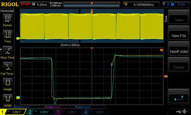 We can clearly see the fast edges of the IR2110 and the totem pole output is a little slower. Notice that there is nearly identical duty time between the two. looking closer, we see more details. 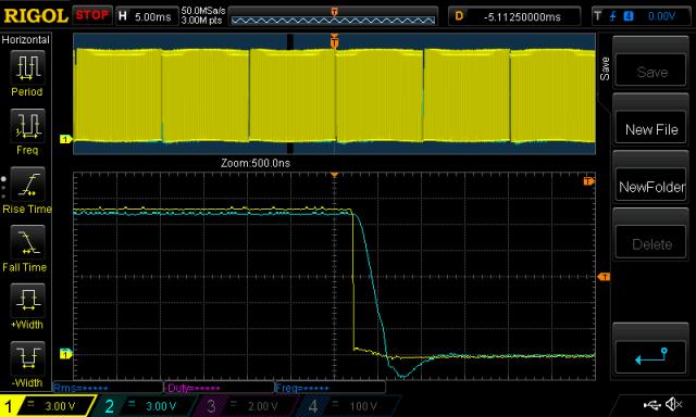 for the left side of the first capture, and 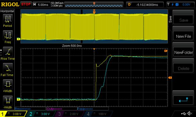 for the right side. Certainly a little slower rise times. But look at the HY4008 specs: rise times are specified. Turn on and off times are of the order of 20-40nS. I suspect the "slowness" of the totem pole design is not an issue, it's fast enough even when using the TIP41/42 combo. Is there any evidence of shoot through? This is completing the post I did just before, so as to include Mad's boards. Light Blue is low side gate voltage (Vgs) Dark Blue is high side Vgs 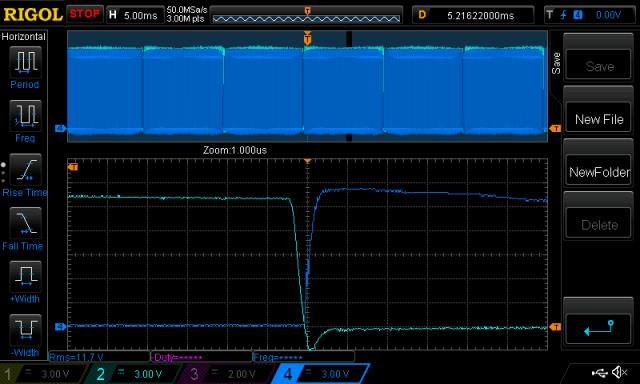 No evidence I can see. It looks great. And the inverter ran nearly silent. Another example 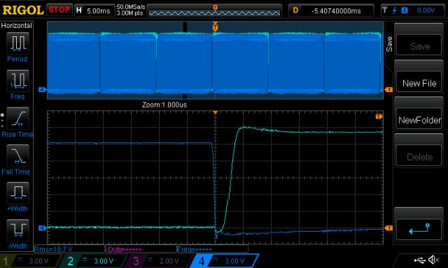 Where ever I looked I keep seeing these clean gate voltages with no little low side pulses as seen in the previous post of mine. This is the best I have seen so far and I can't see how it could be improved. Maybe a little fast rise times from low to fully ON, so as to minimise the switching losses, but this is good. It should come as no surprise that this combo of Mad's power board and his control board runs with the lowest idle current of the lot. 0.30A Once I fit more MOSFETs to the board I expect to see some oscillation and possibly some shoot through start to appear. This effect of multiple MOSFETs using the same gate drive is something for future investigation. I have already blown off a couple of Drain or Source pin pads on this board, from the 2 "whoopsies". Time to get out the solder wick braid for high current repairs. wronger than a phone book full of wrong phone numbers |
||||
| poida Guru Joined: 02/02/2017 Location: AustraliaPosts: 1392 |
Part 31-C: A powerjack control board driving Mad's power board. For completeness, I now run the Powerjack control board against the Mad power board. Yellow is low side gate drive, at the MOSFET pin. Blue is high side gate drive, at the pin. 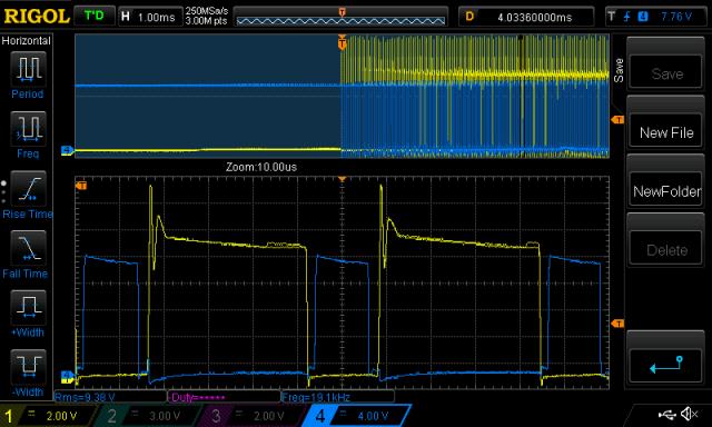 It looks to have a bit of overshoot on the low side rising edge. closer.. 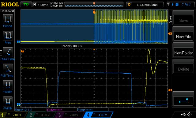 Clearly some sort of overshoot and ringing. This might be a result of the PJ output driving a different impedance now. The PJ controller is designed to drive opt-couplers, not the totem pole as fitted to the Mad board. Notice the 2uS dead time. No shoot through at all, and the idle current was 0.37A When the nanoverter is driving this board, the idle is 0.31A The dead time is hard to determine due to the slower rise and fall times. Maybe 500-800nS? Here is the gate drive voltage from the nanoverter. 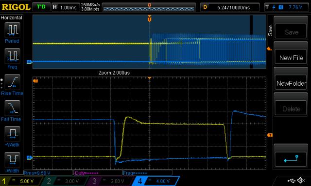 wronger than a phone book full of wrong phone numbers |
||||
| poida Guru Joined: 02/02/2017 Location: AustraliaPosts: 1392 |
Part 32: Ferrite bead on MOSFET's leads Anybody who has opened up a Powerjack LF inverter will see there are tiny ferrite beads on the Drain pins of the low side MOSFETs, on both 1/2 bridges. The Low side Drain pin is of course that which is connected to the output of the inverter board, leading to the transformer primary winding. In operation, this output (and also, the low side FET's Drains) are pulled down to DC supply ground or pulled up to DC supply positive. (pinout for those who might need it) 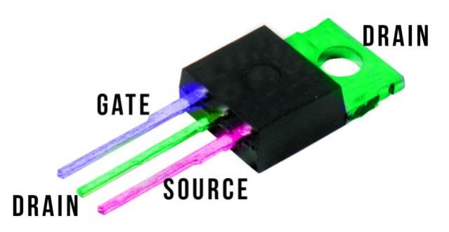 In previous posts I have gassed on about "dv/dt" more than somewhat. This post assumes you are across dv/dt and understand cross conduction or shoot through causes and why it needs to be avoided. RenewableMark gave me a handful of rather large ferrite beads a while ago. It's time to see what they do. First I set up a simple test to show the effect of one bead on a fast enough rising edge. I put a 1Mhz 2.5V p/p squarewave into a 47 Ohm load and see what effect the bead has. As it happens it has profound effects depending on where you put it in relation to the oscilloscope pickoff point. White trace is just the squarewave output across the 47R load. 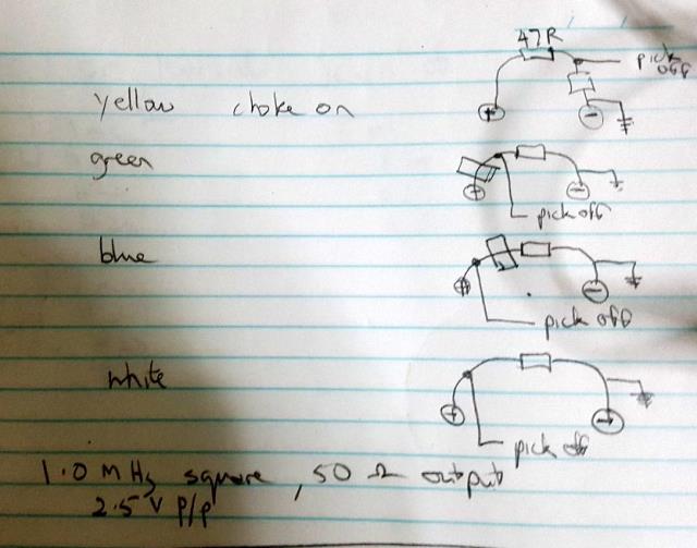 the results: 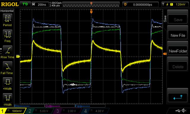 The test set up: 27V DC supply, into the Mad power board with one HY4008 on each leg. Same old primary choke, toroid and 10uF cap on the secondary into zero load. I am driving it with the nanoverter. I placed one ferrite bead on the low side MOSFET's Drain. I left the other low side MOSFET as is, with no ferrite beads. Now we compare the gate voltages of LOW and HIGH during switching and see if there is any effects due to the bead. Looking at a time in the AC waveform, about 15% into the sinewave which is 1.5ms from zero crossing, I find on my test inverter oscillations and cross conduction. Here is the unmodified switch event, when the LOW side opens (i.e. gate goes to zero) and HIGH side switch closes, pulling the output to DC supply. The unmodified 1/2 bridge Yellow is low side Vgs, Blue is high side Vgs 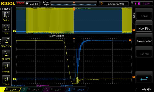 The other 1/2 bridge I chose to add the bead to the Drain. First, UN-modifed. Looks like the other one. And so it should. Light Blue is low side, Dark Blue is high side 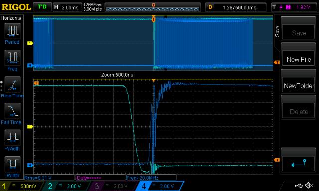 And after the addition of a bead on the Low side FET Drain 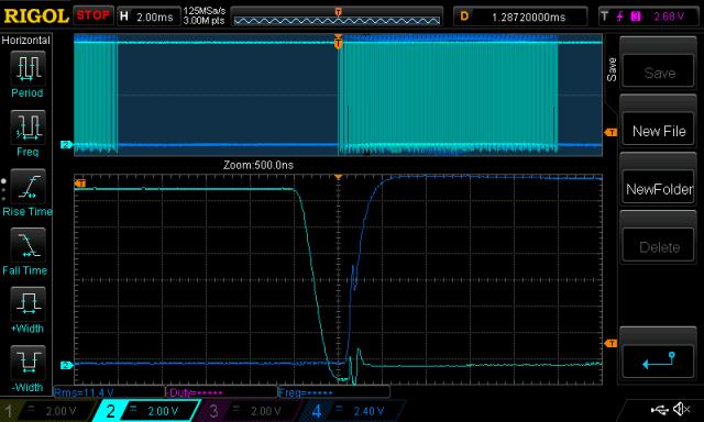 This I can only describe as a huge change to the oscillation. Both the low and high side gate voltages are profoundly altered. Undoubtedly I will be using these beads in any future builds. The particular ferrite beads Mark gave me are very conductive and large in size, so big that they can touch both the Drain and Gate or Drain and Source pins when installed. The DMM reads about 400 Ohms when you touch one side and the other. When I installed the bead, I used some shrink tube to insulate things. The two DSO captures are the same switch event in both cases. Possibly it's the 25th cycle of the 200 PWM cycles that make up the half wave. So much for the low side MOSFET and a ferrite bead. Might there be any advantage in fitting beads on the high side FETS? There certainly is some oscillation remaining. 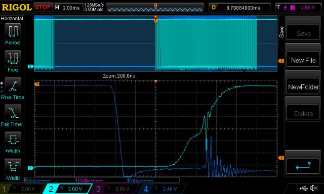 I leave this for the next post. Any views on which pin I should place the bead? (Gate, Source or Drain?) My guess is high side Source pins. wronger than a phone book full of wrong phone numbers |
||||
| wiseguy Guru Joined: 21/06/2018 Location: AustraliaPosts: 1017 |
My guess is the gate will have the best effect - will be interesting to see what unfolds. When I was playing with beads on my setup the upper Drains made no difference. If at first you dont succeed, I suggest you avoid sky diving.... Cheers Mike |
||||
| noneyabussiness Guru Joined: 31/07/2017 Location: AustraliaPosts: 506 |
What about adding the beads to both the drain (on mosfet) and on gate at diode/resistor, so room to fit... ?? I have a ton of different types if you want some for testing poida ?? I have a heap scavenged from various old tvs etc. .. I think it works !! |
||||
| poida Guru Joined: 02/02/2017 Location: AustraliaPosts: 1392 |
I probably wont place any beads on the Gate. The switching speed slows down too much. I would like to get some of the salvaged beads you have. wronger than a phone book full of wrong phone numbers |
||||
| wiseguy Guru Joined: 21/06/2018 Location: AustraliaPosts: 1017 |
Peter I have great respect for all the work and effort you are putting into helping others and their understanding of inverter functioning etc. The Nano1 code is in my opinion the biggest advancement in these forums since I first started reading here. I note that on a few occasions you have said that adding inductance to the gate is detrimental to switching speed and dispensing with the idea forthwith. This is at odds with most application notes that advise to add inductance or resistance or both as required to stop paralleled mosfet oscillation. They also advise that keeping inductance on the source lead to an absolute minimum and always below the value of Drain inductance. This recent App note from Toshiba in 3.2.1 page 7 explains the cure and the preamble why. In 4.2.1 page 15 it describes single FET oscillation with increased source inductance. App Note If you are referring to a large inductance on the gate slowing down switching speed I concur, however my experience has found that some small value of inductance in the gate for paralleled mosfets can be very beneficial and should have little effect to switching speed. Whilst discussing paralleled FET's the same application note describes that the Vth or threshold voltage of the gate is much more important when matching FETs for parallel operation than matching RDSon. Their conclusions are that the FET with the lowest Vth turns on first and turns off last and isnt into sharing the current nicely with the other FETs as they hog all the current themselves during on & off. Keeping switching speed fast and matching Vth looks like a beneficial move to avoiding stressing individual low Vth FETs. If at first you dont succeed, I suggest you avoid sky diving.... Cheers Mike |
||||
| noneyabussiness Guru Joined: 31/07/2017 Location: AustraliaPosts: 506 |
Poida, pm me your address and ill send ya a heap... ill try and sort em right for you.. I think it works !! |
||||
| Warpspeed Guru Joined: 09/08/2007 Location: AustraliaPosts: 4406 |
This is the Holy Grail ! We need to add some deliberate series gate resistance, if only to limit the peak charging and discharging current to something that the driver can reliably tolerate. That resistance should provide sufficient damping to discourage any ringing provided there is also absolutely minimal inductance involved. If the gate driver physical layout is tight, we want absolutely minimal inductance in both the source and gate circuit to discourage ringing. Ringing is particularly bad both from the clean switching aspect, and EMC radiation. The only reason anyone would deliberately fit a ferrite bead to anything is if it fails an EMC radiations test. Slipping on a ferrite bead as a band aid measure might just get it to pass for compliance. So the production guys are given a big bag of ferrite beads and told to fit one wherever it seems to have the greatest effect. Ferrite beads are NEVER designed into something as part of the original design process. Its always a desperate final fix where a big bunch of ferrites of different size and material are tried one after the other to get something to pass mandatory testing. If its designed right in the first place, ferrite beads should not be required. Things always ring for a reason, and its always best to fix the problem at the source rather than trying to damp it out by adding a lossy ferrite bead. Cheers, ĀTony. |
||||
| mackoffgrid Guru Joined: 13/03/2017 Location: AustraliaPosts: 460 |
Poida, Great post. I'd expect a ferrite bead on the upper Source could upset the Gate voltage reference. (btw - I used the new diff probe this week, thanks for the review) Cheers Andrew |
||||
| poida Guru Joined: 02/02/2017 Location: AustraliaPosts: 1392 |
Oh, good to see you have the diff probe. Did you get the DP-25? <Arthur Weasley: from when the boys took the enchanted car for a spin to pick up H.P.> ...how'd it go? The diff probe I mean. I am really pleased with mine. Just what you need when looking at things with non-ground level reference. Agreed that playing with the Source on the upper FET might do bad things. Something must be able to be done to dampen these oscillations. What, I wonder. Slower switching means more time one or the other FET spends too much time conducting through the lossy body diode. I want to continue with the assumption that fast switching times are to be retained as a primary aim. wronger than a phone book full of wrong phone numbers |
||||
| poida Guru Joined: 02/02/2017 Location: AustraliaPosts: 1392 |
I tried a little while back a ferrite bead on the gate, between the gate resistor/diode node and the FET gate pin. This was on the test inverter with 4 x TO220 IRxxxx MOSFETS on each leg. That is, there was 4 FETs sucking up the gate drive, with ample reasons why there was oscillation. It slowed the switching down a large amount. I did not make a post on this test. I probably will do a post on putting a bead on the Gate of the test Mad power board soon. Each test costs a HY4008 and another de-solder/solder cycle. This test inverter has only one HY4008 per leg, so there is no paralleling of FETS going on. Eventually I want to see how a single FET with best drive and ferrite bead arraignments compares with a paralleled setup. First things first. See what can be done to reduce the high frequency oscillations that are fed into (or sent out of) the high side FET Gates. I plan to include also the Vs node voltage (i.e. the primary winding connection point) in the DSO captures, I think this will provide me with some insights that I clearly need. wronger than a phone book full of wrong phone numbers |
||||
| Tinker Guru Joined: 07/11/2007 Location: AustraliaPosts: 1904 |
OK, so from a practical point of view, just how would you go about to select matched Vth mosfets from, say, a bunch of 50 devices. A simple diagram and what to measure where would be great  . .Klaus |
||||
| mackoffgrid Guru Joined: 13/03/2017 Location: AustraliaPosts: 460 |
Poida, Yes I got the DP25. (from a New Zealand mob) A very good decision. I agonized over the cost - its almost half as much as a Rigol Scope. It works very well. Its already helped me. Now I just need to talk myself into trading my 2ch Owon in for a 4ch Rogol. |
||||
| Warpspeed Guru Joined: 09/08/2007 Location: AustraliaPosts: 4406 |
This is actually a very easy test to do Klaus. Connect the gate directly to the drain, and fit a pullup resistor to a voltage source. Or you can just use a constant current power supply to do it. The gate and drain voltage will rise up together to the gate threshold, and the mosfet will then act like a shunt voltage regulator at the gate threshold voltage. The choice of pullup resistor and voltage source sets the current at witch the threshold voltage is being measured, and that will be the same for every device tested, so its excellent and very repeatable for comparative testing. Cheers, ĀTony. |
||||
LadyN Guru Joined: 26/01/2019 Location: United StatesPosts: 408 |
what is a good way to test the voltages across the MOSFETs - for example Vds, Vgs etc? I have many DMMs that have an input impedance of around 1MOhm - and they dont read the Vds, Vgs properly due to loading. For example, my Vds readings are only accurate once Rds is in the kOhm range so that the DMM loading effect is reduced - otherwise, when the Rds is comparable (or higher) than 1MOhm, the readings are completely misleading! What's a good way to handle this (besides getting a DMM with a much higher input impedance)? |
||||
| Warpspeed Guru Joined: 09/08/2007 Location: AustraliaPosts: 4406 |
If you are doing the gate threshold test at 100mA or 1 amp or something, then multimeter loading is going to be negligibly small. Cheers, ĀTony. |
||||
renewableMark Guru Joined: 09/12/2017 Location: AustraliaPosts: 1678 |
Interesting Tony, when I get a machine running even though the mosfets get rds matched one or two always run hotter (10-15c above the others with laser gun test) so I snap them out and replace them and then they have run at the same temp as the others. That Vth might explain it.  Cheers Caveman Mark Off grid eastern Melb |
||||
