
|
|
Forum Index : Microcontroller and PC projects : General purpose I2C IO module
| Author | Message | ||||
| flasherror Senior Member Joined: 07/01/2019 Location: United StatesPosts: 159 |
You might want to have a 3 pin /RE jumper to select between: 1. /RE is active all the time (meaning the MX170 receives all transmissions, including its own) i.e. /RE which is grounded and only DE is under program control. 2. /RE and DE both connected so can only listen to RS485 bus when not transmitting. The reason is sometimes it is useful to see all transmissions on the RS485 bus (for example using as a bus monitoring device). Also make sure the PCB can fit a 0.5W (half watt) resistor for the "ground current limiting" resistor (might be Rg on the PCB?) considering the surrounding components. I would also add a 3 pin male header near the RS485 connector as an alternate RS485 bus connector, or use as test points for the RS485 signals (same A/B/GND). And: RX/TX LEDs so can see bus activity PCB version # on silkscreen Change bi-color LED to two single LEDs if PCB space allows (just my opinion). Edited 2022-01-12 23:39 by flasherror |
||||
| Mixtel90 Guru Joined: 05/10/2019 Location: United KingdomPosts: 5726 |
I'm not happy about changing the R/G LED to separate ones. It won't happen on my design. Every bit of something that leads to the outside world is another problem in locating it in the end plate. A single LED is at least 5 times easier to line up than two. :( As it is I'll have a single end plate that works with both the I2C and the 485 versions. The current version is designed to give two modes of operating DE. As standard Pin 7 is inverted to provide the signal. To use direct connection Q1 is omitted, together with RB. A link is fitted where shown on the circuit board and the 10k collector resistor RU is transferred to the RG position to force the system into receive by default. The user must then raise pin 7 prior to transmit and lower it once the TX buffer is empty. There is no "ground current limiting" as it's not required here. I think TXD and RXD would normally both sit at 3V3 and the LED is a common anode type, so you could probably connect the resistor side of the LED14 link and the GND end of the red LED resistor to TXD and RXD. The resistor values limit the current to approx. 3mA through the LED. That would give you pure hardware LED drive. This *is* the pcb. There's unlikely to be any further changes (by me anyway). I didn't originally intend to make a RS485 version at all. :) Mick Zilog Inside! nascom.info for Nascom & Gemini Preliminary MMBasic docs & my PCB designs |
||||
| flasherror Senior Member Joined: 07/01/2019 Location: United StatesPosts: 159 |
Agree with the mechanical concern about using the same plate. The problem is that it cannot be configured to "always listen" to the RS485. Without a schematic I cannot easily understand the design (A bit off topic but I am amazed by people who can layout a design without a schematic - easier to have an integrated schematic & board for me). Most RS485 designs have a low value resistor to limit potential currents through ground as a result of connecting multiple RS485 devices together. This resistor is between RS485 ground pin and the board ground trace. Is your ground trace directly connected to the RS485 ground terminal? What is "Rg" resistor for? It's up to you whether further changes are done, but not having the RS485 LEDs rules out using this for me (which is understandable if you ever had to troubleshoot RS485 without having the benefit of signal status LEDs  ) )Edited 2022-01-13 02:23 by flasherror |
||||
| Mixtel90 Guru Joined: 05/10/2019 Location: United KingdomPosts: 5726 |
I2C version circuit diagram: 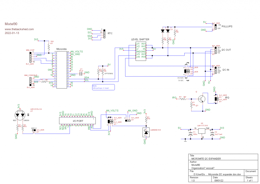 RS485 version circuit diagram: 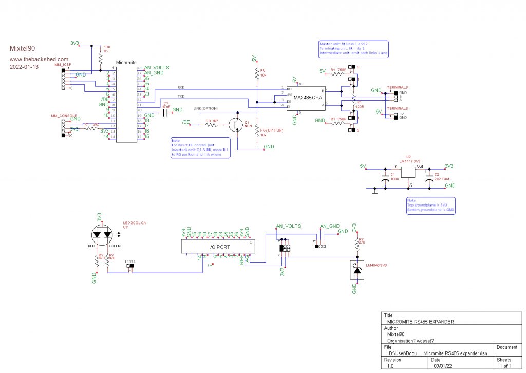 Please remember that these are not to be used for "serious" things like machine control. They are learning/hobby exercises and there is no protection from external problems or anything like that. I'm not going to produce devices for commercial use under any circumstances - under UK law I would be personally liable if something went wrong due to malfunctioning of one of my devices. Hence, if you find that I've omitted things that you'd expect on commercial gear then I'd respectfully suggest that you purchase proper equipment rather than try to use these as the manufacturer will (hopefully) be covered by suitable insurance. Sorry, I can't produce rear views of the PCBs in SL6 as it doesn't allow you to display them in construction mode or print them in Photoview mode. Note that all tracks in blue are on the rear of the board. Mick Zilog Inside! nascom.info for Nascom & Gemini Preliminary MMBasic docs & my PCB designs |
||||
| Turbo46 Guru Joined: 24/12/2017 Location: AustraliaPosts: 1593 |
That looks good thanks. I agree that Rx/Tx LEDs (under the cover) would be nice but it's not a deal breaker for me. Do they still make logic probes? Maybe the demo version can display the rear side? It's a little difficult to see what's on the rear. Maybe a disclaimer on the board? Bill Keep safe. Live long and prosper. |
||||
| Mixtel90 Guru Joined: 05/10/2019 Location: United KingdomPosts: 5726 |
On the rear of the RS485 version I've just gone for a horizontal male pin header for the link block, simply taking 0, 2 or 4 links. This can be a vertical type if you want to keep the links inside. The two and 3 way terminals have 1mm square pins on 5.08mm centres. You can use fixed terminals, vertical pluggable terminals or horizontal pluggable terminals (as shown on the drawing). The I2C version uses horizontal male pin headers all along the back. The IRQ one has two rows and is intended to take two Dupont connectors horizontally one above the other, one as a loopthrough and the other to the host. They are simply in parallel. I still have my old Realistic logic probe. :) When you can get a cheap little Chinese logic analyser it seems silly though - it simply reads serial data as text on the PC screen. :) Mick Zilog Inside! nascom.info for Nascom & Gemini Preliminary MMBasic docs & my PCB designs |
||||
| Turbo46 Guru Joined: 24/12/2017 Location: AustraliaPosts: 1593 |
Some thing like this? Mounted on the rear? Not the top? Vertical ones on the top will do for me I think. Bill Keep safe. Live long and prosper. |
||||
| Mixtel90 Guru Joined: 05/10/2019 Location: United KingdomPosts: 5726 |
You went and did it, you lot, didn't you? I was determined to leave this board alone and you gave me the challenge to fit more bits onto it - and I couldn't resist. :) 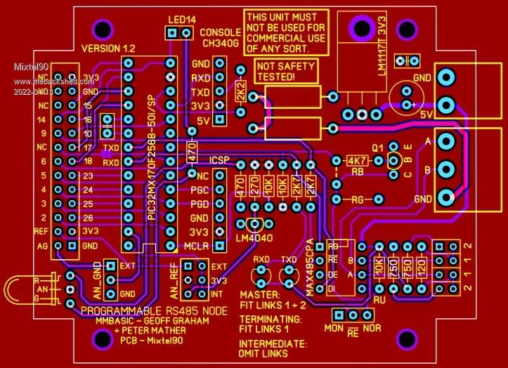 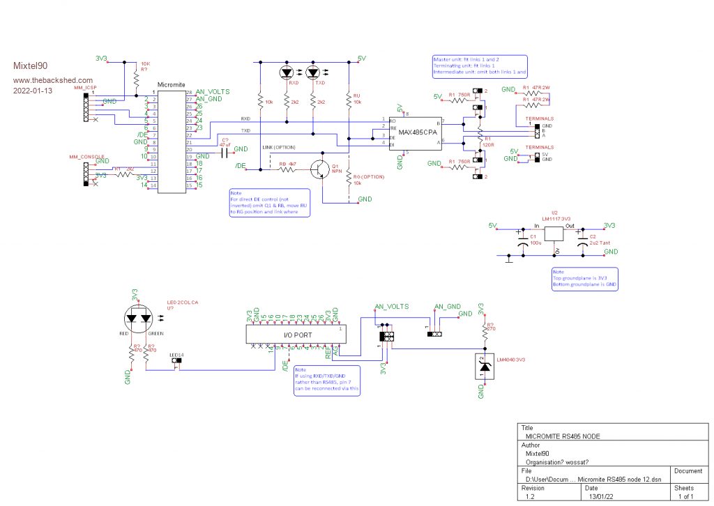 Mick Zilog Inside! nascom.info for Nascom & Gemini Preliminary MMBasic docs & my PCB designs |
||||
| Turbo46 Guru Joined: 24/12/2017 Location: AustraliaPosts: 1593 |
 Looks good. Thanks. Looks good. Thanks.Small question: on the schematic, should the /DE signal go to the pin marked '7' on the I/O connector? Bill Keep safe. Live long and prosper. |
||||
| Mixtel90 Guru Joined: 05/10/2019 Location: United KingdomPosts: 5726 |
Not normally. There's a solder blob link on the back of the board that can make that connection if you want to forget RS485 and use TXD/RXD/GND instead (easy enough to link out on the pcb). Normally /DE is connected via the inverter to the MAX485. (I've just noticed that I've missed the 2-position link for the MAX485 RE connection off the circuit there...). The normal alternative connection is via the "direct connection". I think /DE on the IO connector is generally a bad idea and just asking for trouble with a RS485 connection. :) EDIT: Shown the missing link now. :) 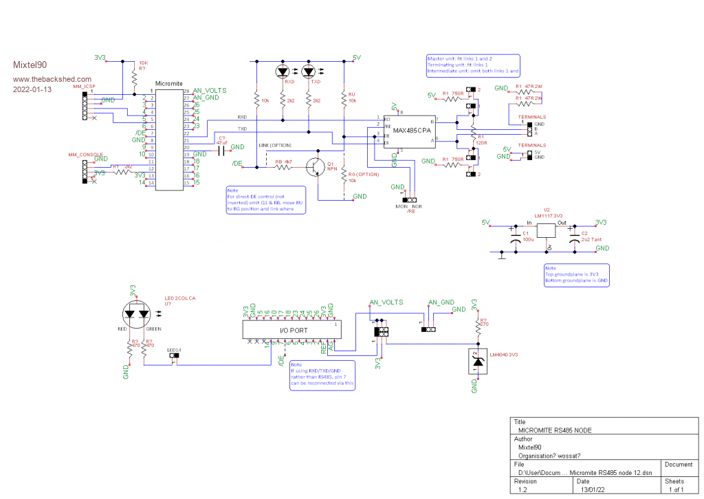 Edited 2022-01-13 22:54 by Mixtel90 Mick Zilog Inside! nascom.info for Nascom & Gemini Preliminary MMBasic docs & my PCB designs |
||||
| Mixtel90 Guru Joined: 05/10/2019 Location: United KingdomPosts: 5726 |
Special Three for Two offer today! Here's a bit of something for those who like to solder. Same size board. Optional regulator and 3.5mm barrel jack for 5V. Same IO connector and LED, all connected to pads on a big sea of holes. Back end open for whatever you want. Note that this isn't a female connector to plug into the male connectors on the other boards - I'm not even sure if you can get them. This board might be nice if you wanted to use a conventional I2C expander chip for all digital signals or perhaps for interfacing from a 20mA current loop. No circuit diagram. It's self-explanatory really. 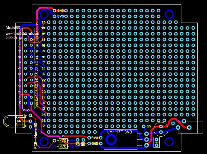 Mick Zilog Inside! nascom.info for Nascom & Gemini Preliminary MMBasic docs & my PCB designs |
||||
| Volhout Guru Joined: 05/03/2018 Location: NetherlandsPosts: 3527 |
@Mixtel, The LM1117 has 100uF at the 5V and 2.2uF tantal at the 3.3V output. The 2.2uF is however the only decoupling cap at the 3.3V rail. There is no 100nF at the MX170. That may be a bit risky, since the LM1117 is not close to the MX170. Maybe the 485 driver could also use a capacitor to decouple the Vdd (5V). Regards, Volhout Edited 2022-01-14 01:33 by Volhout PicomiteVGA PETSCII ROBOTS |
||||
| flasherror Senior Member Joined: 07/01/2019 Location: United StatesPosts: 159 |
Connecting it could be a good test point if you needed it (scope trigger). About the RS485 does anyone else think two ground current limit resistors (the 47 ohm 2 watt in series) are overkill? I think one 100 ohm should work fine. Maybe should have diode on 5V input jack to protect against reverse polarity? Edited 2022-01-14 01:53 by flasherror |
||||
| Mixtel90 Guru Joined: 05/10/2019 Location: United KingdomPosts: 5726 |
@Volhout I did think about extra caps near the MX170, however there's virtually no volt drop and a lot of distributed capacitance between the groundplanes. It's something to think about. You could always pop a 100nF disk under the board if there's a problem. :) The 2.2uF (or a bit more) tantalum is, according to the LM1117 spec (providing I've read it correctly, that is), fine for regulator stability and a bypass isn't needed for that. Note that it can't be an aluminium electrolytic. @flasherror You can connect pin 7 if you want, the option is there. Don't blame me if someone's incorrect wiring screws up your RS485 comms though. :) I'm not putting TXD and RXD on there either, for obvious reasons. In theory someone could make some sort of board that would plug into any of these modules and, no matter how they've wired it, it shouldn't mess up the comms system (unless they've deliberately used the SDA and SCL lines on the I2C module). Hence I'm not having a permanent connection to pin 7 on the 485 module as this is a normal IO pin on the I2C version. You can use one, two or no ground protection resistors. If you are looping a common 5V supply through then you don't want any - fit a link. If you have 2km of cable between them with 30 more nodes then 94R 4W might not be enough - you may need 100R 7W mounted off board. You can use 100R 0.5W if you like, it's no problem. There just happened to be board space available to take them. They are an option. :) If you are clever enough to solder the bits on the sea of holes I expect you to be clever enough to at least check the polarity of your supply and get it right first time. :) This isn't a beginner's module as it doesn't do anything. (It's more fun to put a 10A reverse biased diode across the jack so it blows up the PSU if you get it wrong. :) Doesn't have any volt drop either.) Edited 2022-01-14 02:29 by Mixtel90 Mick Zilog Inside! nascom.info for Nascom & Gemini Preliminary MMBasic docs & my PCB designs |
||||
| flasherror Senior Member Joined: 07/01/2019 Location: United StatesPosts: 159 |
You and I have very different ideas of "fun"  |
||||
| Mixtel90 Guru Joined: 05/10/2019 Location: United KingdomPosts: 5726 |
Yes. :) I've suffered from that in the past. Now I know how to infuriate people. :) I've just checked the LM1117 datasheet. The output cap should be 10uF tant minimum, so ignore my decimal point and use 22uF. :) Don't know where I got 2.2uF from. I was looking at other regs at the time though, so it may have been one of those. Mick Zilog Inside! nascom.info for Nascom & Gemini Preliminary MMBasic docs & my PCB designs |
||||
| Turbo46 Guru Joined: 24/12/2017 Location: AustraliaPosts: 1593 |
I think I was reading the schematic incorrectly. It looked to me that '- - -/ DE' connection was going to pin 6 on the I/O connector. I used to be indecisive but now I'm not so sure. Not really sure about the resistors in series with the RS485 connector. In my opinion (and experience) that pin should be only used for earthing the shield and the shield should only be connected at one end. Those resistors may compromise the shielding. It may be OK to connect both ends of the shield in a light industrial or home setting (I wouldn't). We used RS485 to connect to switchyard equipment in high voltage electricity substations where an earth fault in the yard could have disastrous effects. I do realize they can be optional. Thank you for the 'sea of holes' board. I haven't checked whether a mating connector is available for the I/O connector but one could be made by using two rows of single pin headers. Depends if the height of the components on the 'motherboard' would allow that. Bill Keep safe. Live long and prosper. |
||||
| Mixtel90 Guru Joined: 05/10/2019 Location: United KingdomPosts: 5726 |
I've been playing again anyway. :) I've included space for an internal header for Gnd/RXD/TXD monitoring. In line with a Circuit Cellar article: I've made it a single 100R 1W resistor for ground protection. The 750R balancing resistors have been reduced to 560R. Interesting to note that if you use CATn cable to connect them then you get a better match using 100R terminating resistors than using 120R (although the drivers are expecting 120R). Mick Zilog Inside! nascom.info for Nascom & Gemini Preliminary MMBasic docs & my PCB designs |
||||
| lizby Guru Joined: 17/05/2016 Location: United StatesPosts: 3015 |
[Posted by mistake on wrong thread.] Edited 2022-01-14 09:13 by lizby PicoMite, Armmite F4, SensorKits, MMBasic Hardware, Games, etc. on fruitoftheshed |
||||
| Turbo46 Guru Joined: 24/12/2017 Location: AustraliaPosts: 1593 |
CAT cable has a characteristic impedance of 100 ohms. That's handy to know if you are pushing the boundaries of speed or distance. An external resistor of 560 or 680 ohms will bring the resistance down to near 100 ohm (+/- 2%) if needed. Regarding the 'balancing resistors' this module uses a value of 20k (R5 & R6) What's next an HC-12 Module?  Bill Keep safe. Live long and prosper. |
||||
